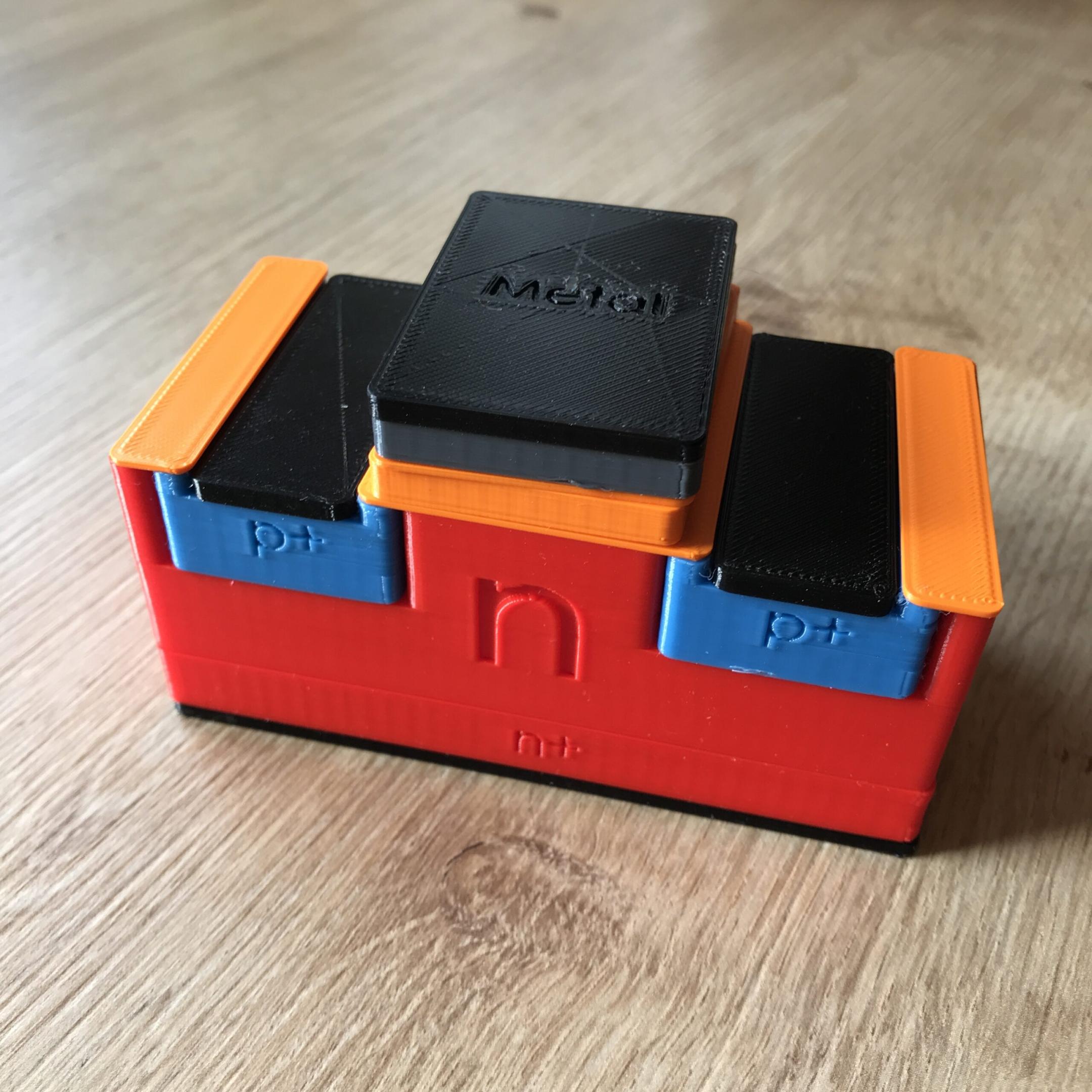
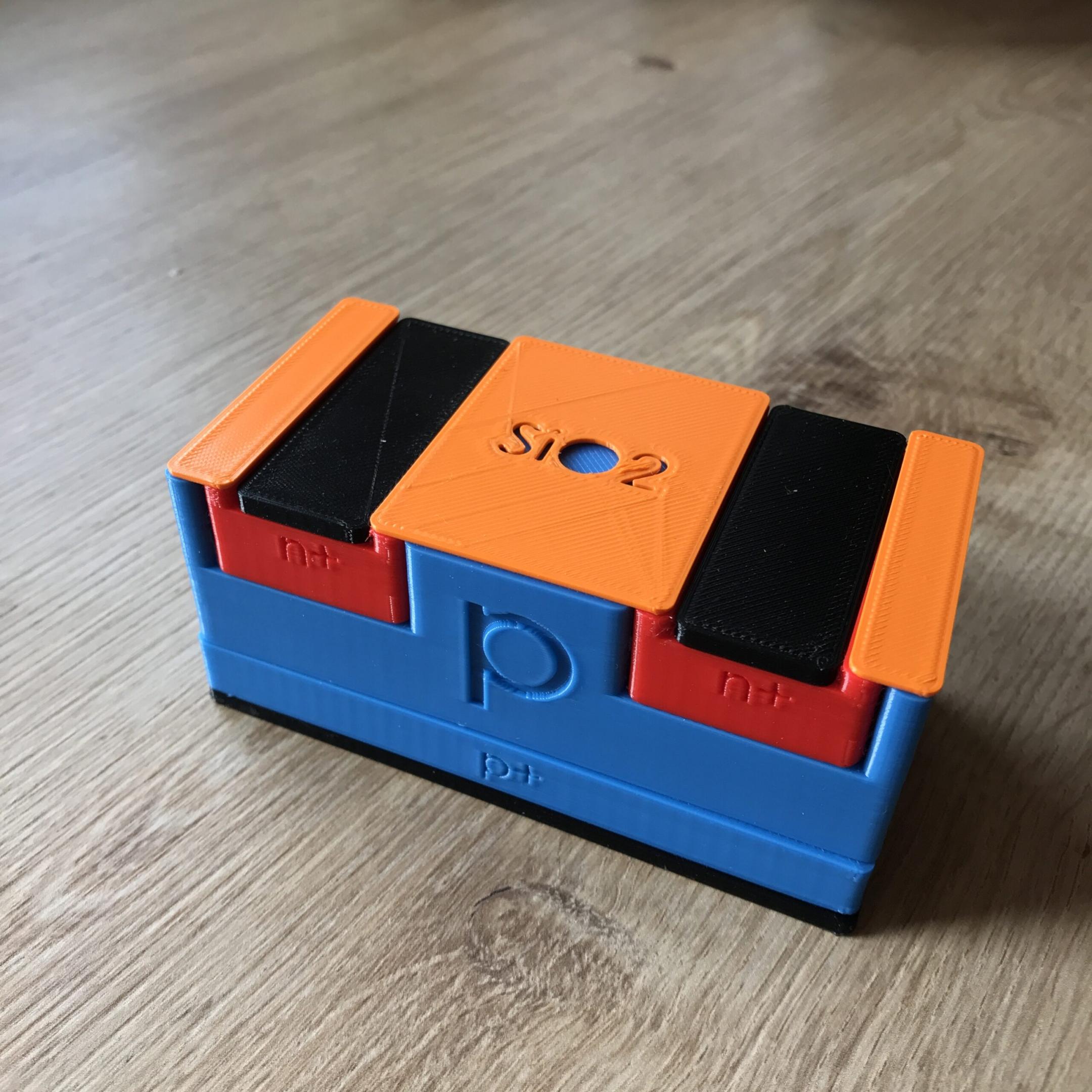
This is a MOSFET 3D puzzle that I constructed in Solidworks and printed it using my Geeetech A10 printer. Both n- and p-channel devices can be built.
Below the final assembly of an n-channel MOSFET can be seen. The dimensions (thickness etc.) may be a bit off when compared to a real MOSFET crossection under the electron microscope.
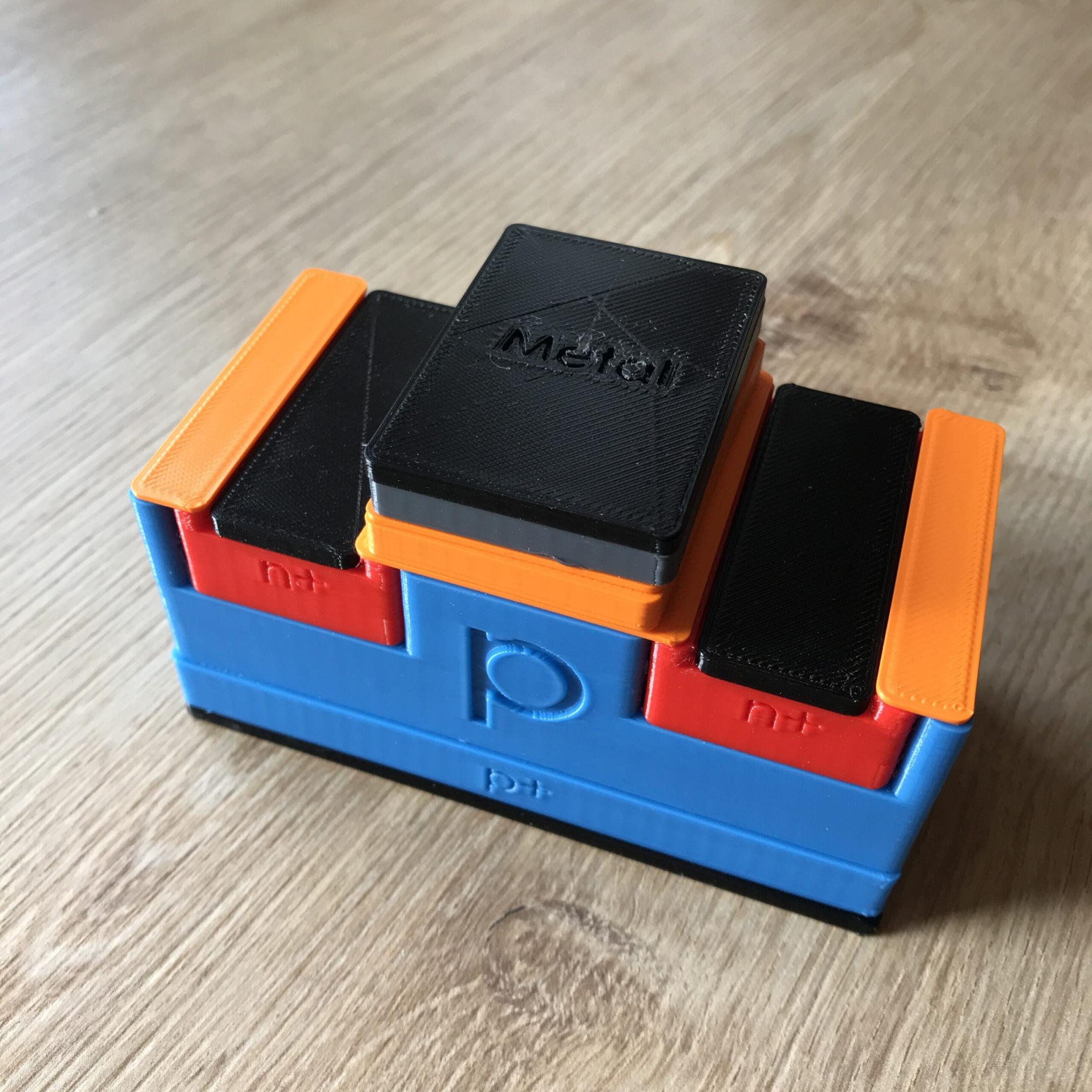
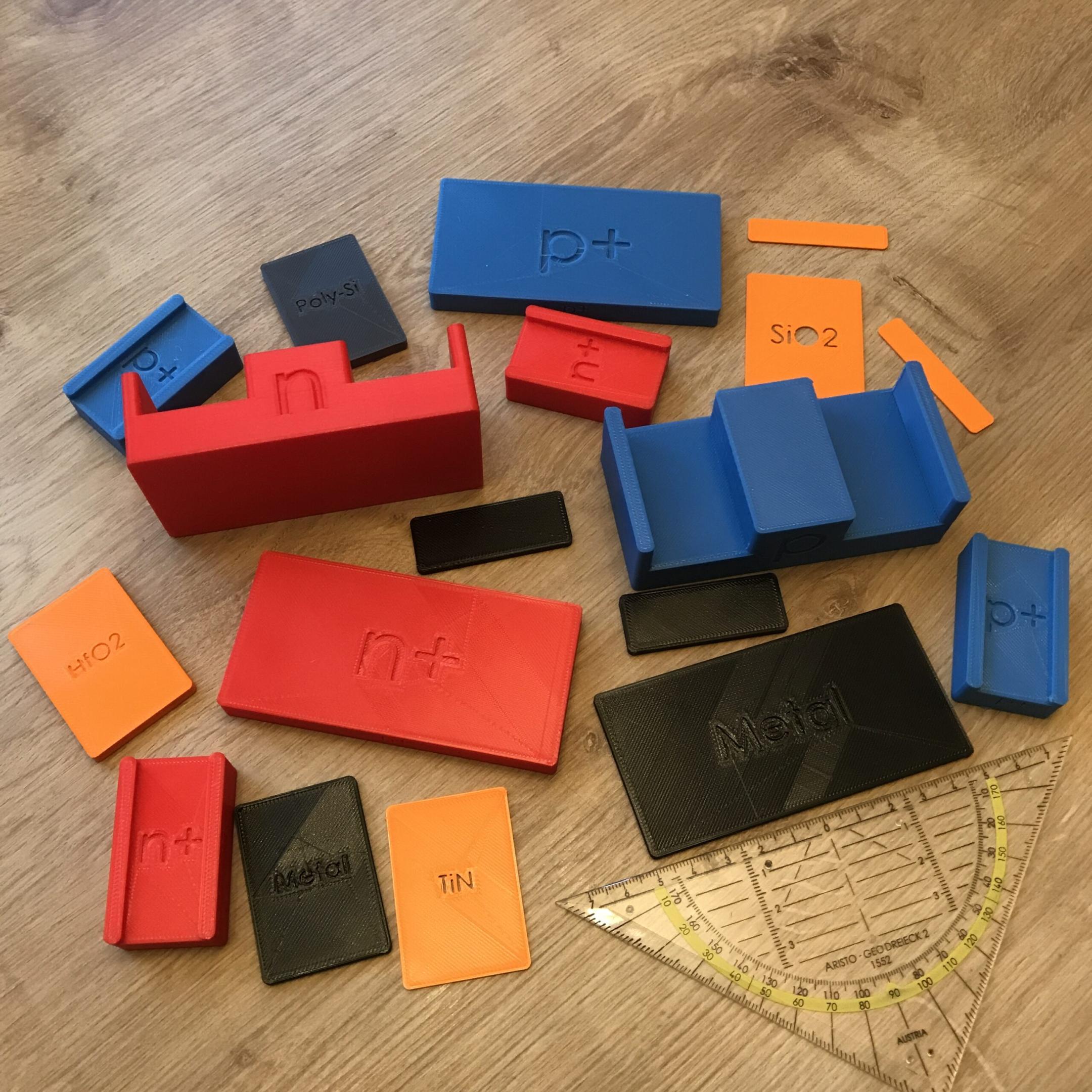
Individual layers and their functionality (n-ch)
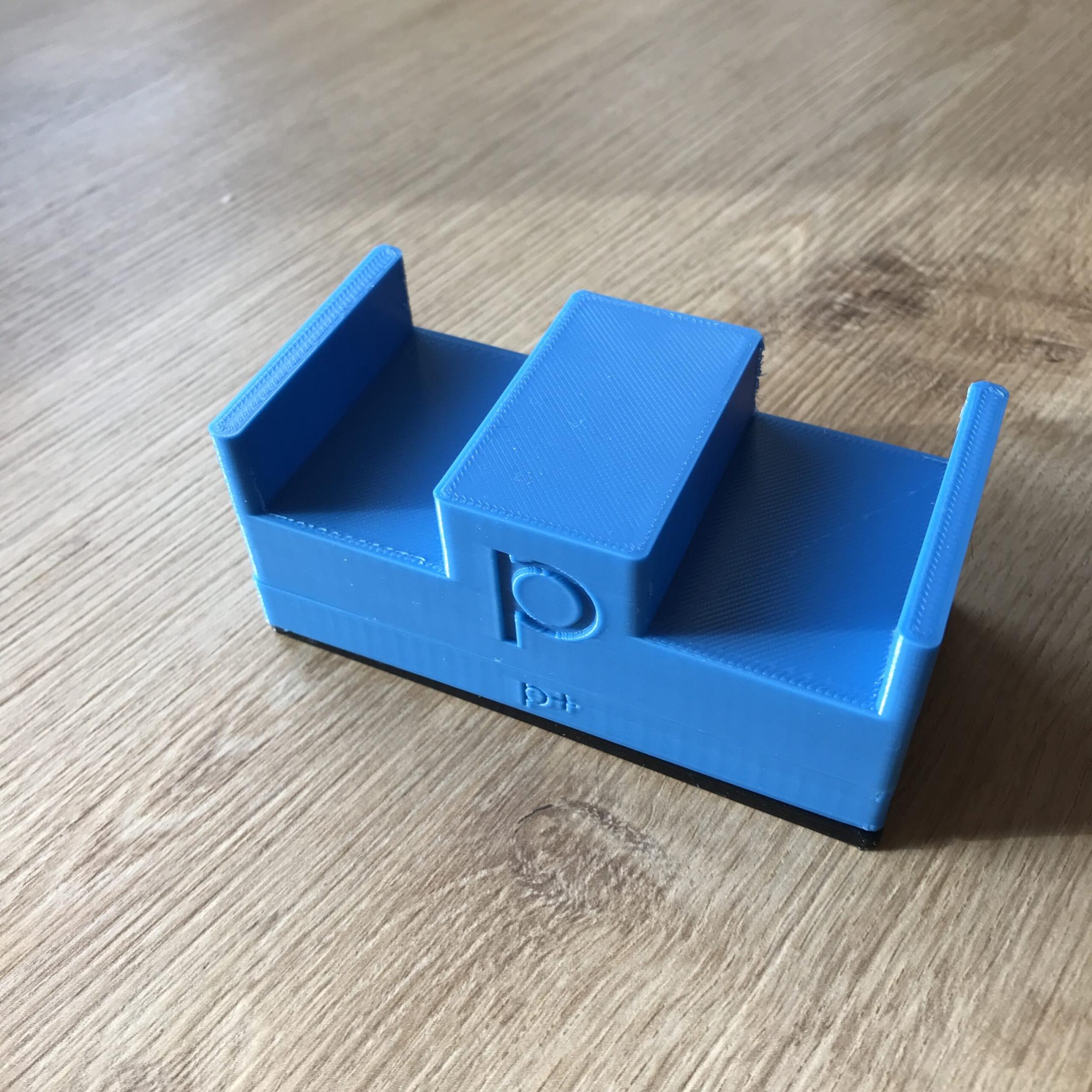
First part is the metal contact for the bulk.
On top of the bulk contact is a heavily doped p-layer in order to form a tunnel contact for a good electrically conducting contact between metal and semiconductor.

Next a normal p-type semiconductor is put on top usually using the epitaxial growth method (same crystal orientation), a layer of crystal is deposited over a single crystal substrate. A Si-Wafer with 100 orientation is the best plane to grow SiO2 on since the atomic planes are parallel to the surface in this case.
In the real manufacturing process, the n+ sections are implemented a bit later but for building this 3D puzzle, they are already stacked together at this stage. The explanation is made when the polysilicon layer is introduced since this layer plays an important part for this matter.
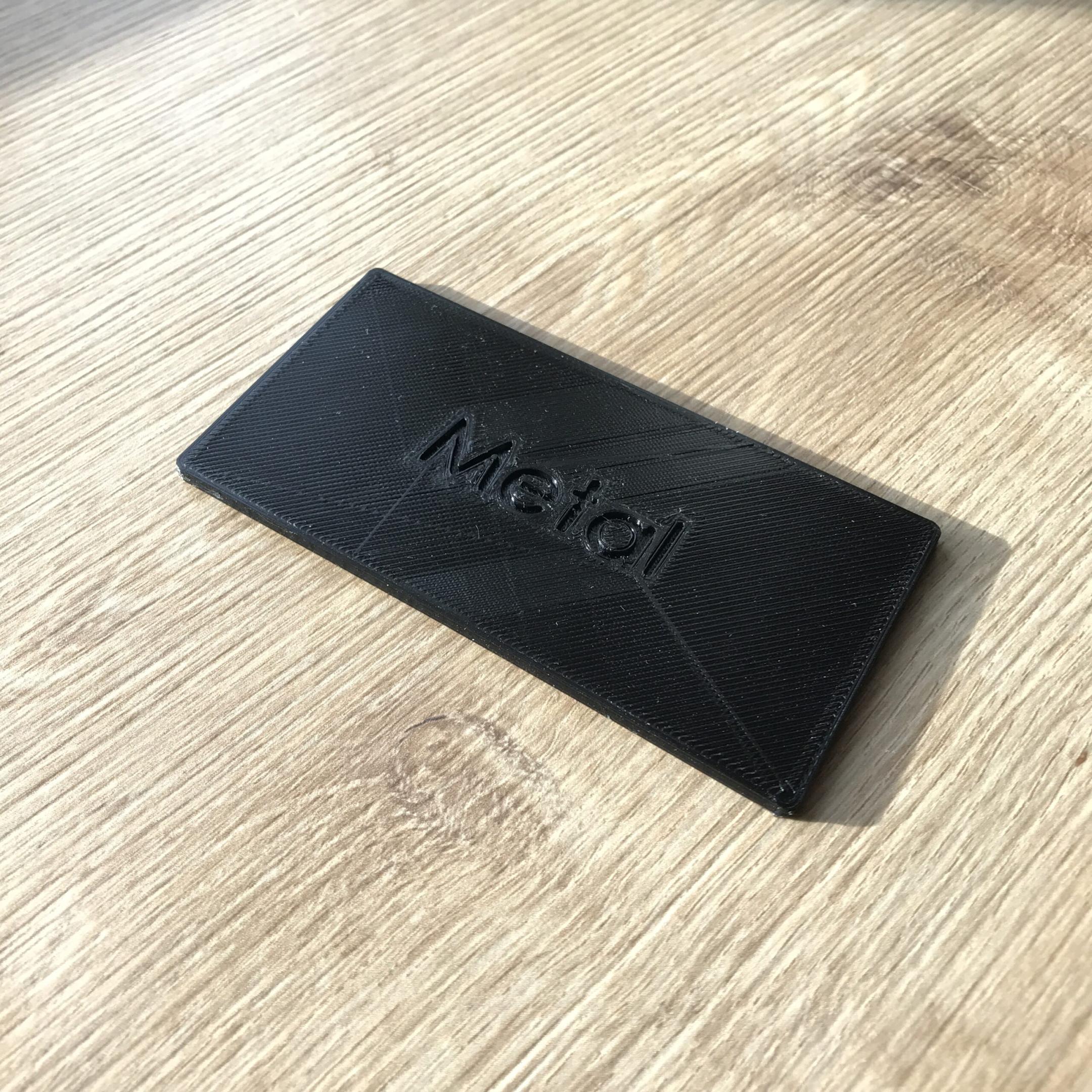
A thin SiO2 layer is created on top. Dry oxidation method is used for this,because it produces very high quality SiO2 layer which are required at the gate. Si is put in atmosphere of oxygen and of high temperature, it creates an oxide from the single crystal and also higher quality oxide than you get by depositing oxide (plasma enhanced CVD).
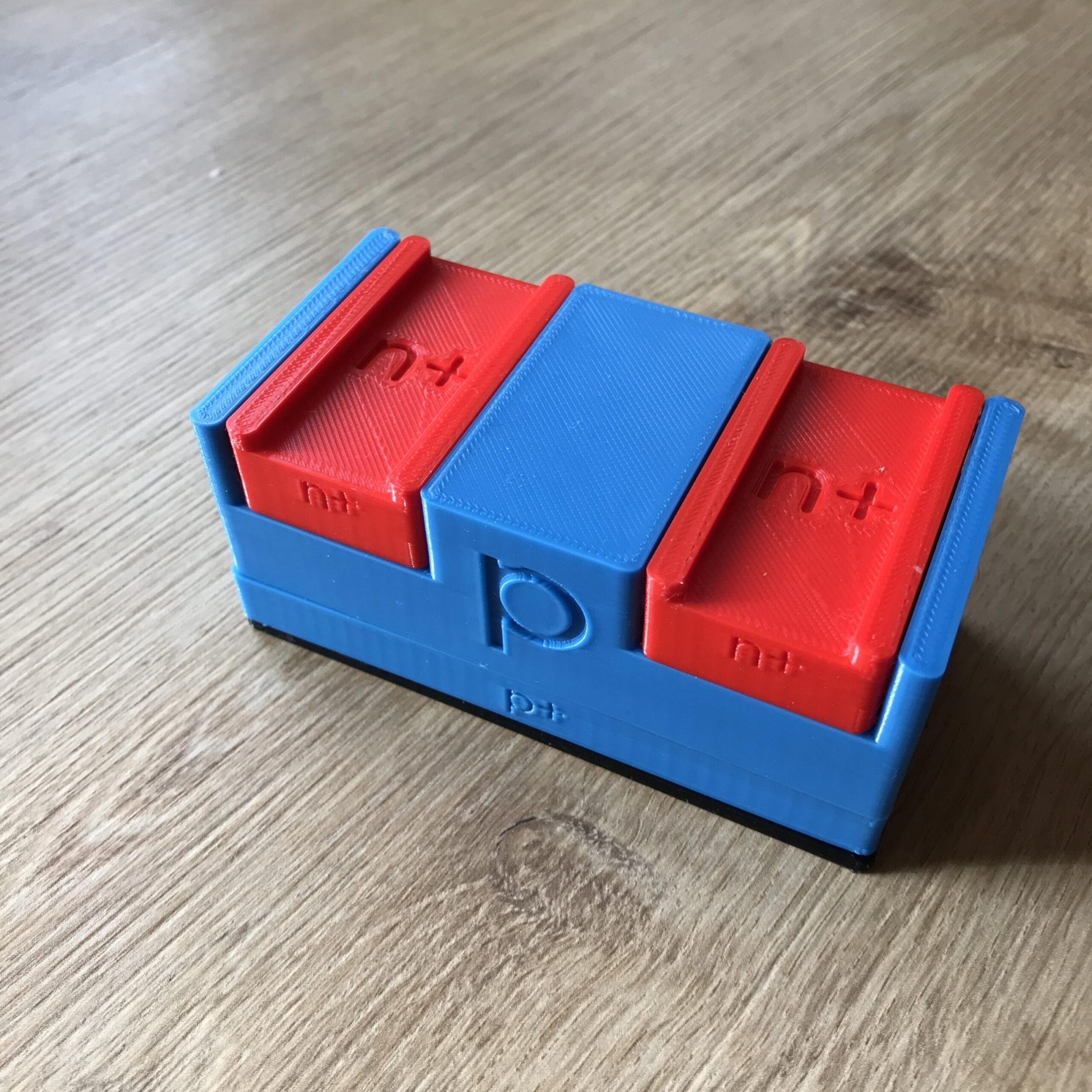
The metal contacts for drain and source are already put into the model but in reality they are implemented at later stage.
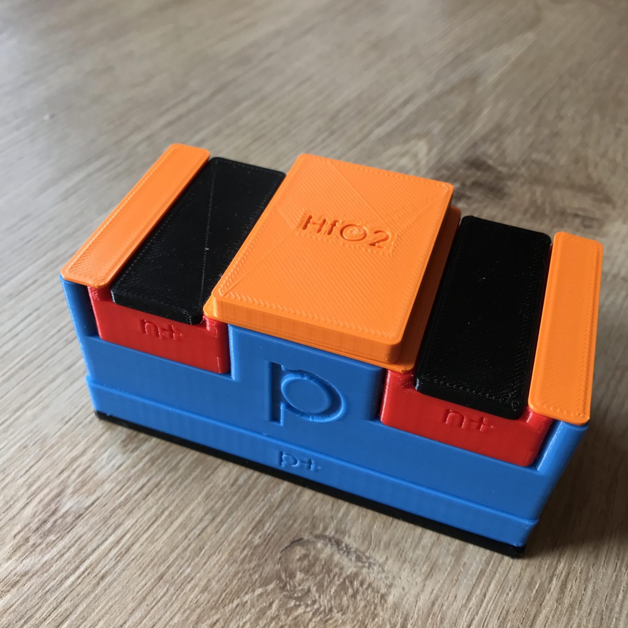
So now it gets more interesting. Hafnium dioxide (HfO2) is deposited on top of the SiO2 at the gate. HfO2 has a high permittivity e_r of around 25, SiO2 permittivity is only around 4. The high e_r is important for the operation of modern devices for low threshold voltages, high gate capacitances and low gate leakage currents. At low supply voltages e.g. 1.2V for CPUs you also want low threshold voltages because otherwise the transistor simply won’t turn on. Using SiO2 alone would be insufficient.
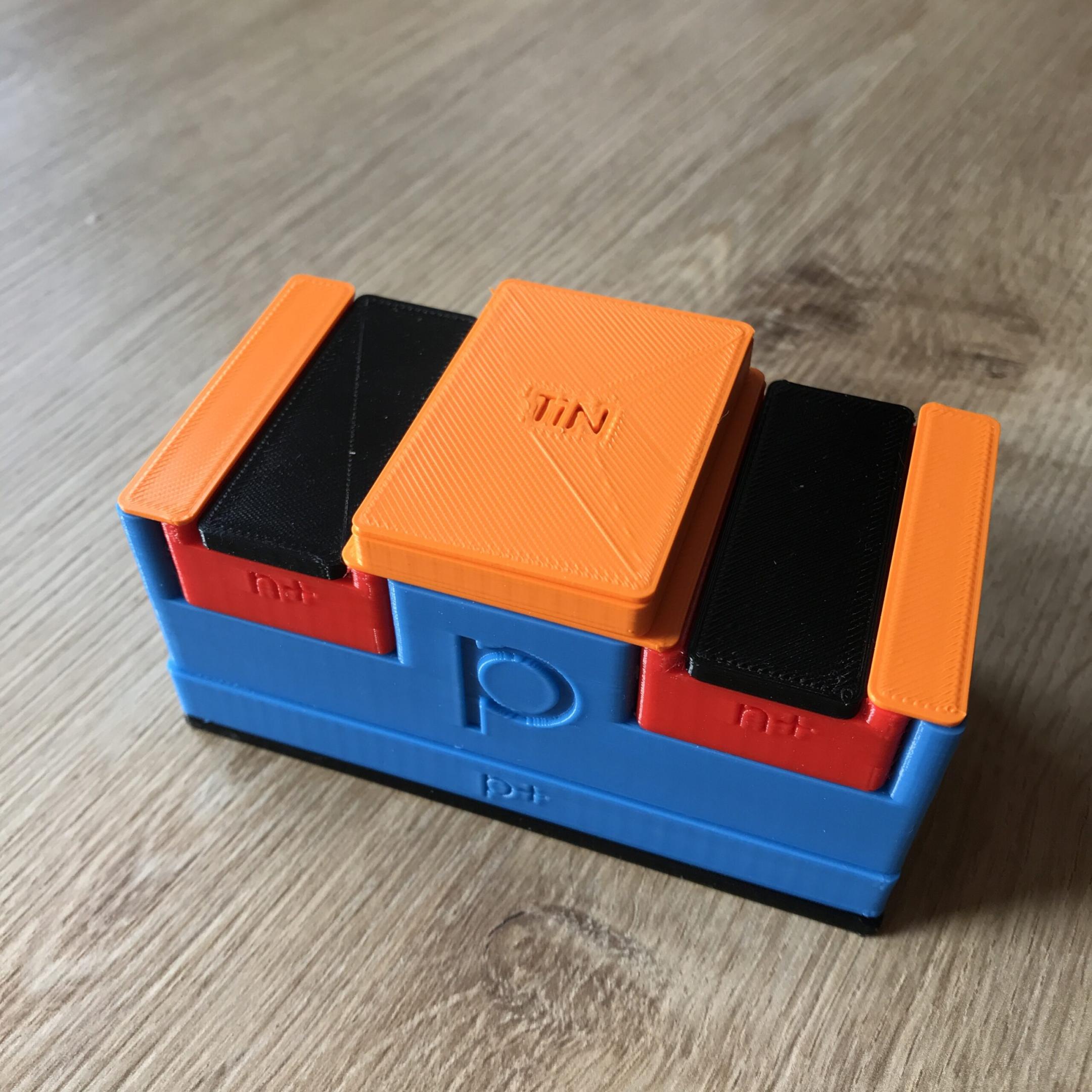
On top of the HfO2 layer a layer of Titanium nitride (TiN, a metal) is deposited. That’s the gold/brass looking coating you often find on drill bits as well. TiN is chosen because it bonds really well with high-k dielectrics like HfO2 and its midgap workfunction. The workfunction is tuneable by varying the thickness of the TiN layer. The good bonding reduces unwanted things like surface trapped charges on interfaces and reduces phonon scattering.
By adjusting the thickness of the TiN layer (nightmare manufacturing-wise), the threshold voltage can be changed, so multiple mosfets with different Vth can be built on the same substrate/stackup.
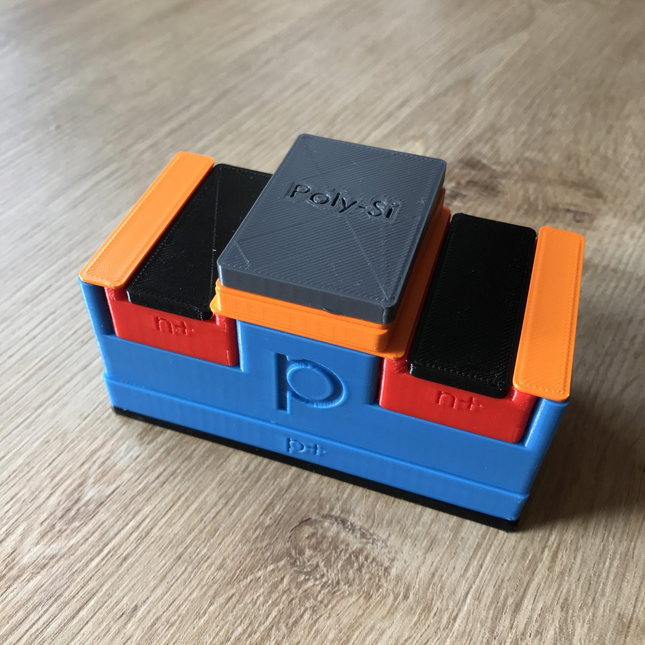
The next step is to apply the Poly-Si layer. Now this layer wouldn’t be required for the functionality of the device since the TiN-HfO2-SiO2-p-Si stackup already makes a good MOS capacitor. The Poly-Si layer is rather used as a mask in the self-aligned manufacturing process. Self alignment is a very good thing, it allows manufacturing very tiny structures.
Now the n+ regions for drain and source are already placed in that 3D puzzle but in reality now would be the time to implement them. This is done by shooting donor ions into the p-Si with the help of the ion implantation technique. The donor ions are blocked by the Poly-Si layer above the gate which acts as a mask protecting the channel underneath, because the channel should remain p-doped.
After that, Silicon nitride is applied on top of everything (no 3D print for this). It also sticks to the side of the gate stackup. Ecthing is done to remove the silicon nictride everywhere except at the sidewalls of the gate stackup. Another run of ion implantation is made to further increase the conductivity of drain and source but this time the donor ions do not flow under the gate so much, since the silicon nitride has kinda widened the gate stackup.
Now, the source and drain areas are established, but the metal contacts are still missing (even though already there in the 3D puzzle). Some transition metal like Titatium (Ti) is is deposited everywhere, then heated up and it forms titanium di-silicide. Silicide is not formed on nitride or oxide. Since Si has a pretty open structure, the TiSi2 goes inside the Si atoms. The rest that has not gone into the Si is etched away. It leaves behind a metallic layer at the gate, source and drain. Again, a tunnel contact is formed at source and drain because of the heavily doped n-Si layer underneath.
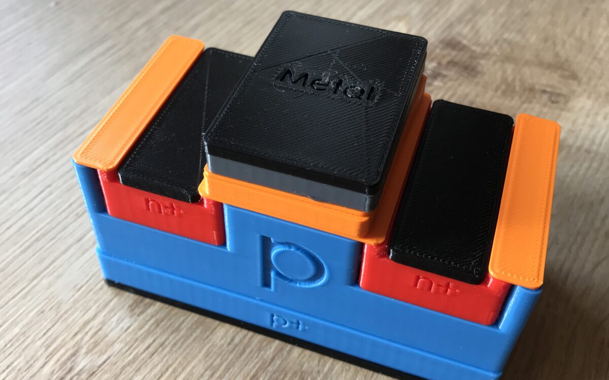
By switching out some blocks, it is also possible to build a p-channel MOSFET instead of an n-channel.