
Switching large capacitances is generally problematic due to the high inrush currents involved. When using MOSFETS to do so, close attention must be paid towards Safe Operating Area (SOA) during turn-on. The inrush current can either be limited by using powerful resistors to charge up the capacitors in a side-branch before closing the contacts on the main current path, or by limiting the rate of voltage rise, since capacitor current is  . A compromise must be found between low
  during operation to minimize
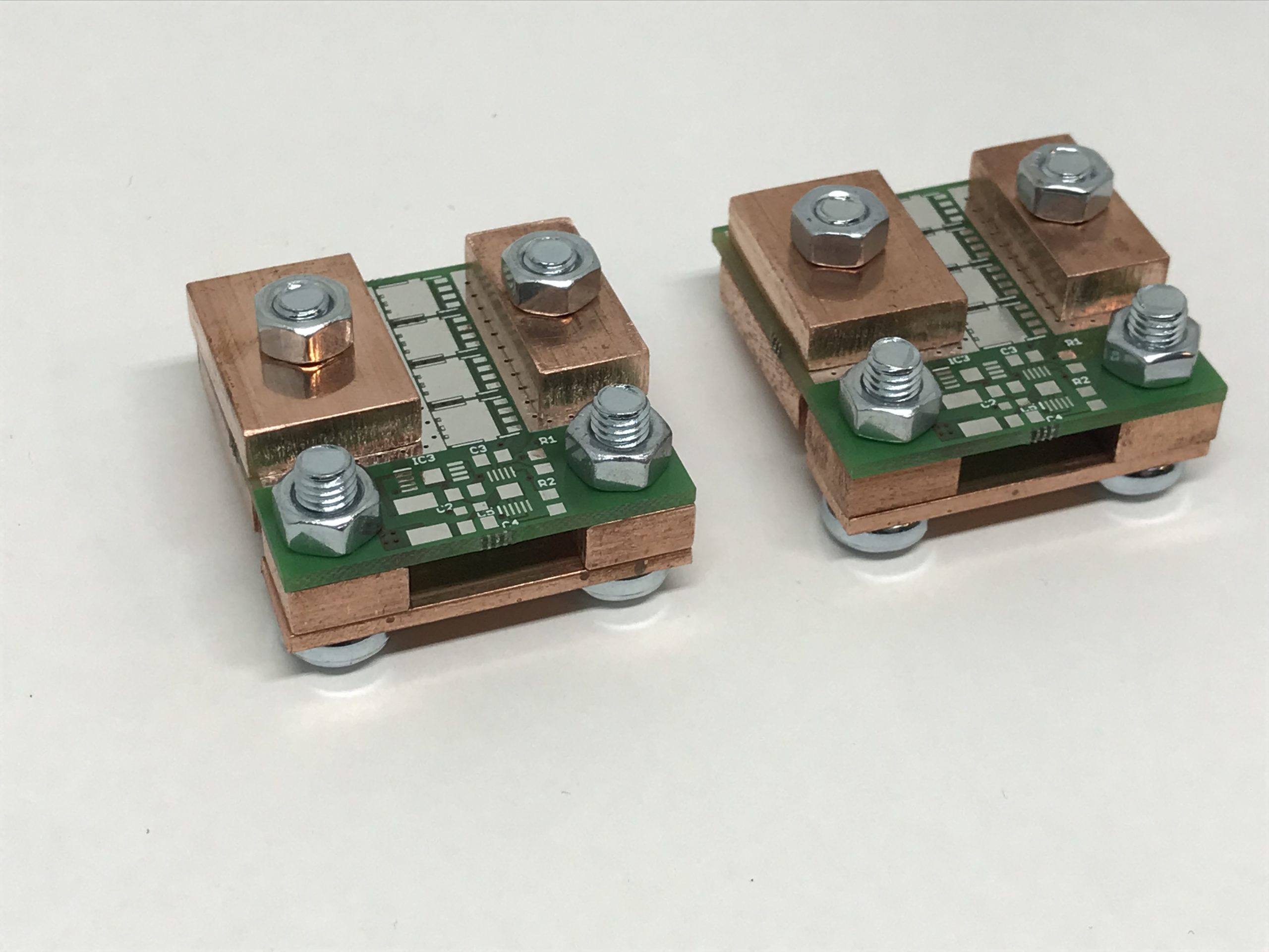
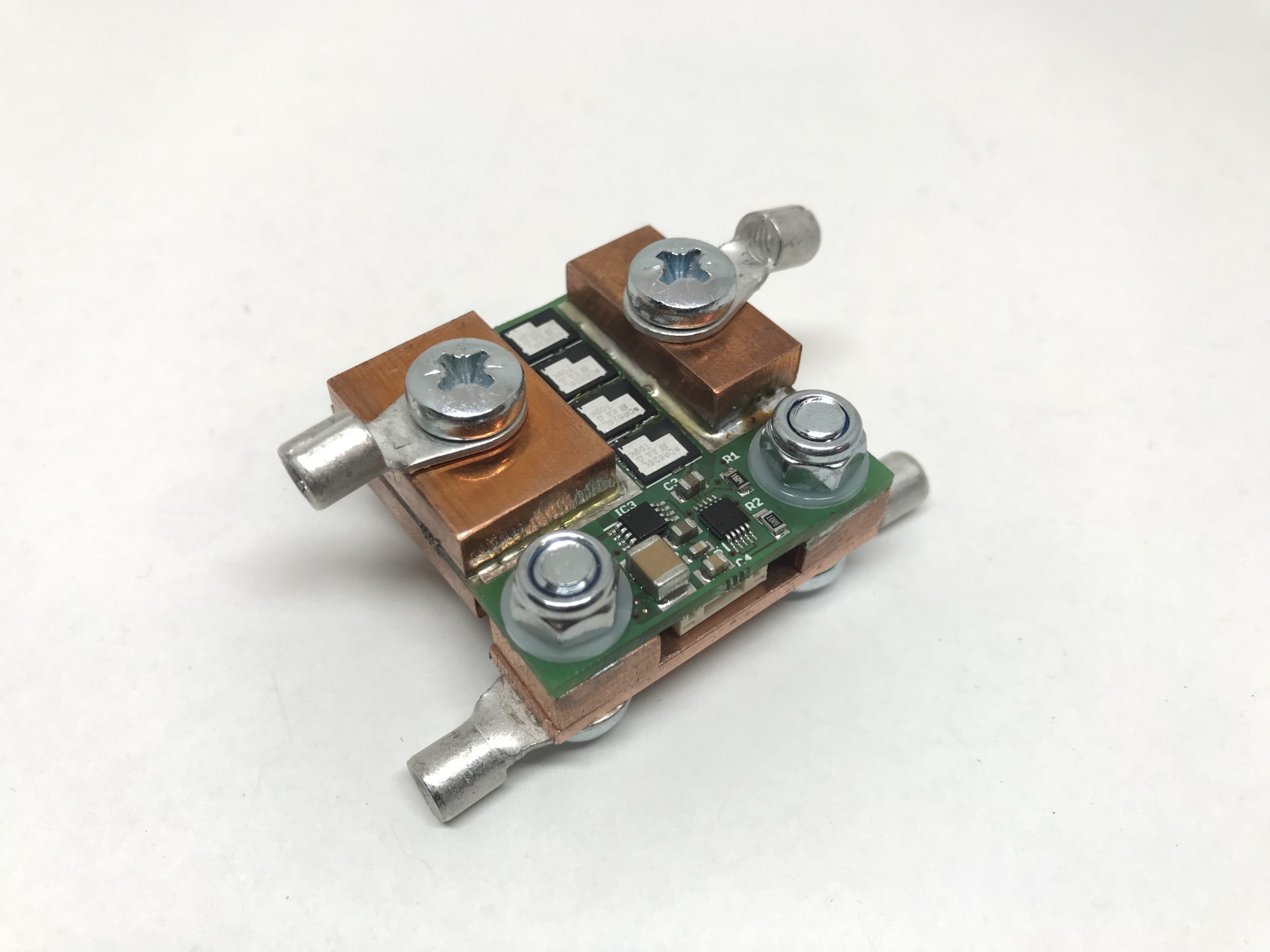
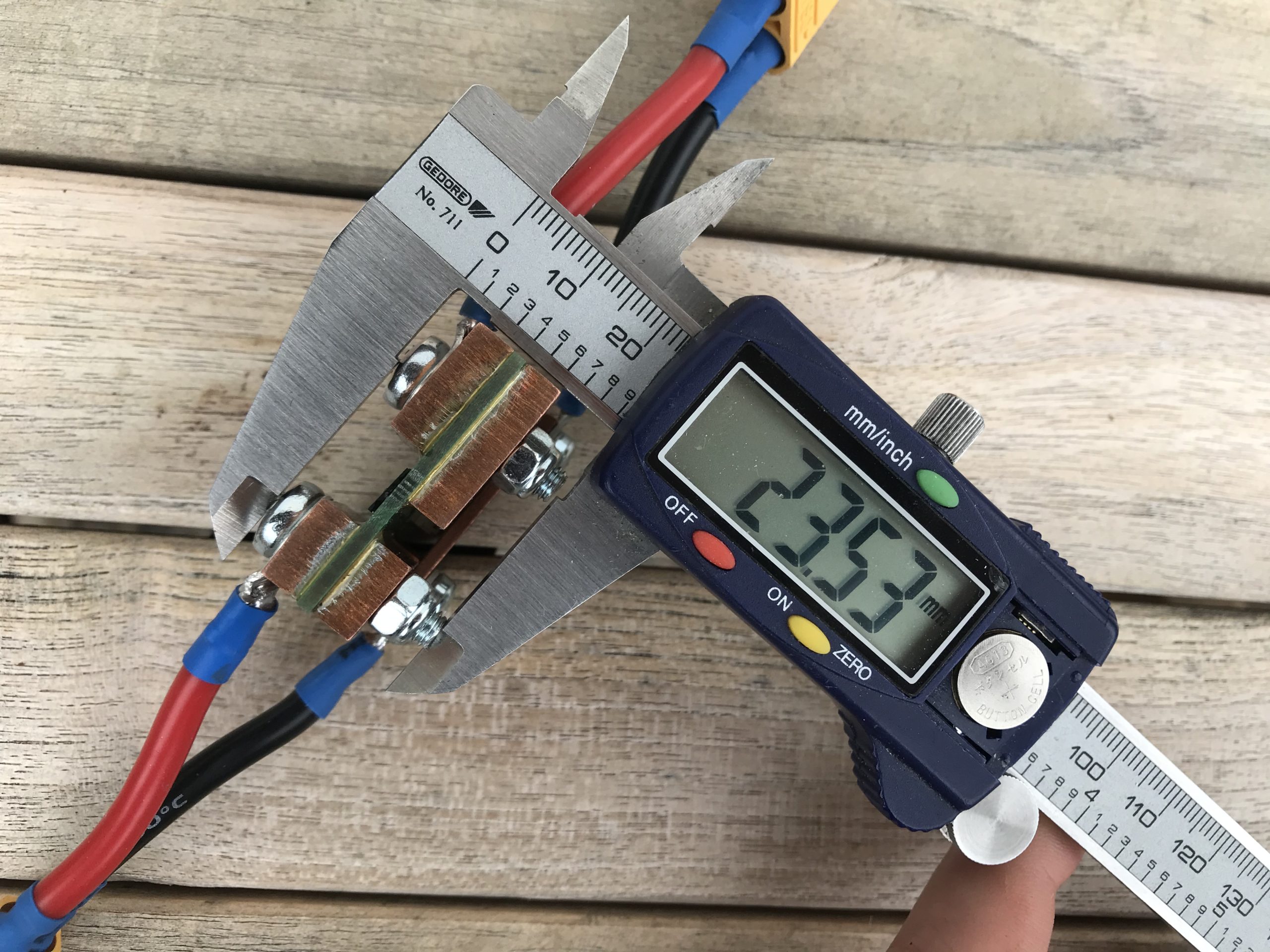
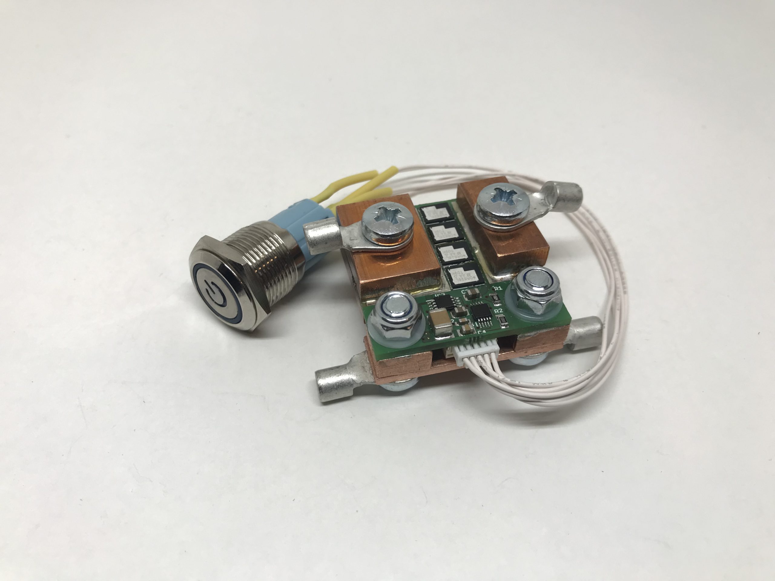
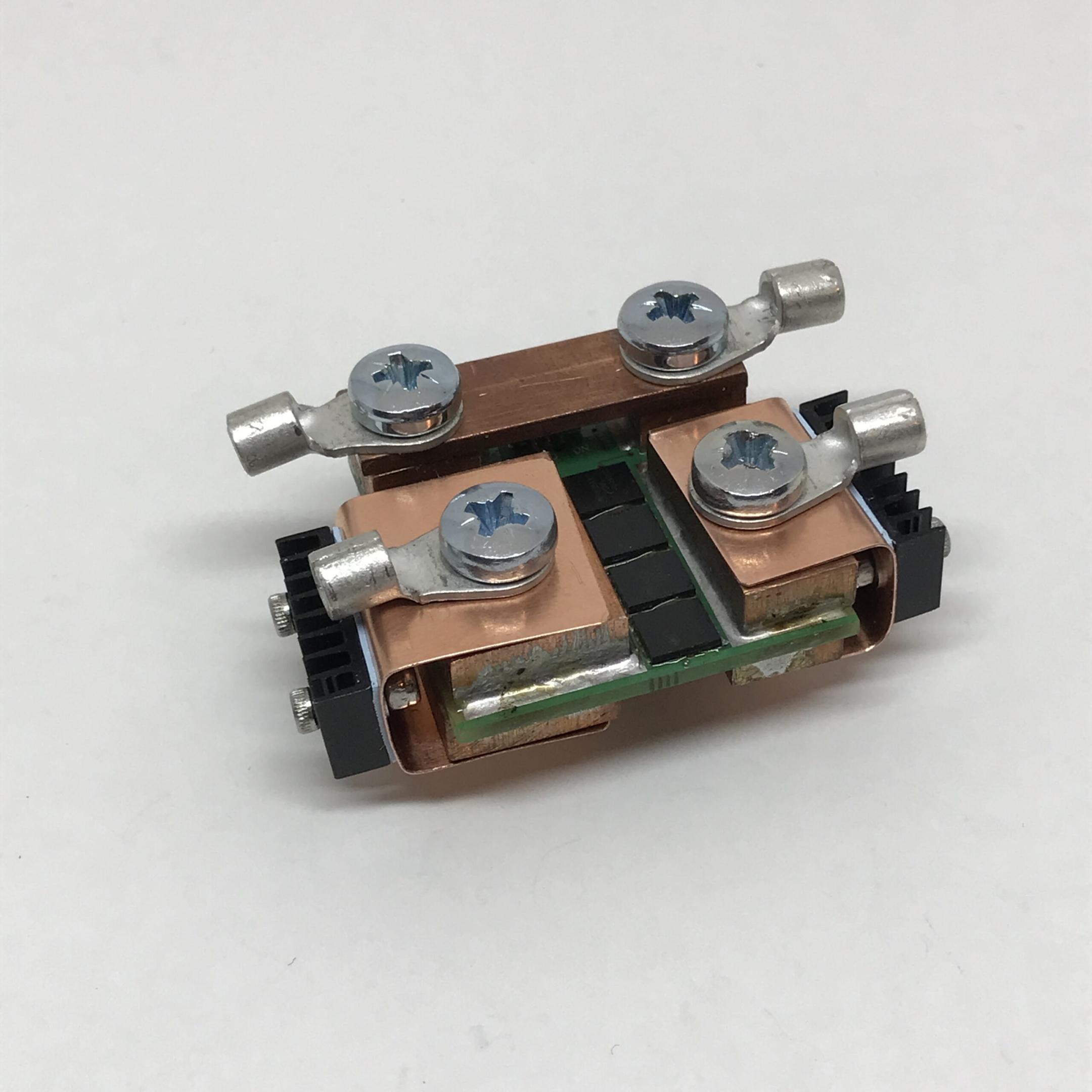
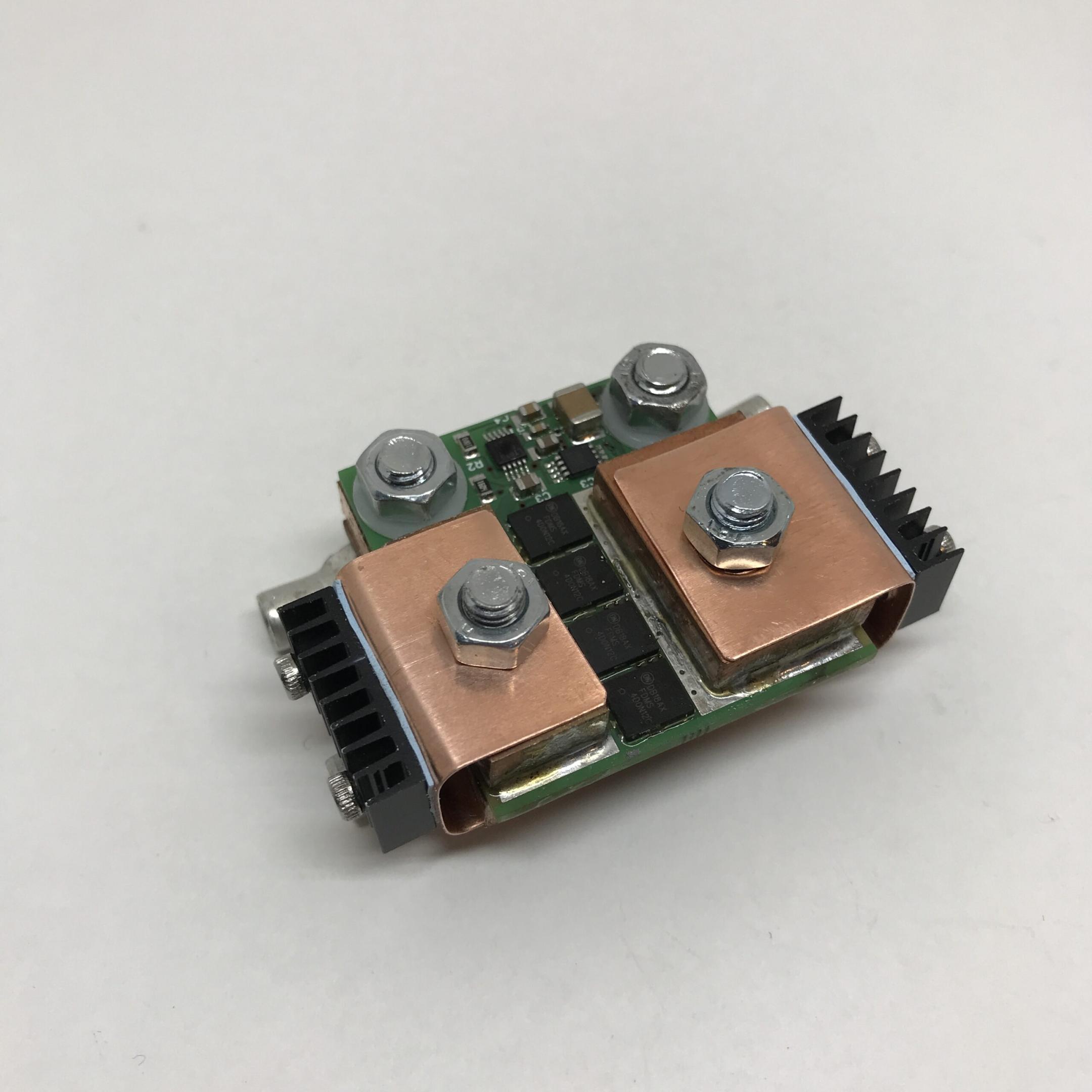
  losses and good SOA behaviour for a safe turn-on procedure. The copper bars combine screw terminals, thermal capacity and massive cross section.
This switch uses N-Channel MOSFETS in High-side configuration and dV/dt limiting for inrush current control.
3D-View from Altium (click and hold to drag it around)
Specifications ScorpionLV v2:
- up to 60V (no more than 12s recommended)
- 175A continuous current*
- up to at least 15 000 uF capacity on output side possible
- latching SPDT illuminated switch for ON/OFF (pressed=ON or pressed=OFF, easy customizable)
- JST-GH (secures connection with a barb)
- M5 screw terminal
- 35mm x 36mm x 23,5mm
- Weight: 90g
Specifications ScorpionHV v2:
- up to 120V (no more than 100V recommended)
- 125A continuous current*
- up to at least 15 000 uF capacity on output side possible
- latching SPDT illuminated switch for ON/OFF (pressed=ON or pressed=OFF, easy customizable)
- JST-GH (secures connection with a barb)
- M5 screw terminal
- 35mm x 36mm x 23,5mm
- Weight: 90g
*number valid for test setup as shown in chapter “Current load capability testing”
It is important to know the limits of the switch and what it is designed for and what not. In the initial moment the power switch is turned on, there must not be any load connected that will draw significant amounts of current besides the capacitors of the load. Once the capacitors are charged, the switch automatically opens fully and large load currents can be drawn.
Therefore, this switch is not suitable to e.g. switch DC heaters (they are basically just a resistor with a ventilator) or PWM dimming a light, because rated current will be drawn immediately. In a typical application scenario, the switch would be placed between a voltage source (battery pack) and a brushless motor controller. Brushless motor controllers do have big input capacitances to cover short-term current peaks and prevent voltage drops during them. When switched on, the capacitors are charged up and after 2-3 seconds the switch is ready to conduct them big currents.


MOSFET selection
Mouser offers around 16 000 different N-channel MOSFETs at the moment. Applying basic search result filters like mounting style, number of channels, maximum Vds, maximum acceptable Rdson, displaying only stocked and neglect NRND and low-stock products narrows it down to about 80 remaining possible choices. Then factors like preferred packages and pricing come into play. Hiding non-stocked ones could sometimes also be a bad idea, as it might be in-stock somewhere else. The advertised current value is a useless marketing number (unless you use liquid nitrogen cooling lol) and only helps a bit to determine if the MOSFET is optimized for low Rdson and high current capability or good SOA behaviour. More interesting is the derating of allowed ID and dissipation power at ambient and case temperatures higher than 25°C, e.g. the switch is inside a shrink tube with no airflow present. Then the advertised big numbers quickly become very small. E.g. 300A down to 30A at 100°C. In addition, those numbers are mostly only valid for certain conditions, e.g. non-repetitive current flow of 10s and 1″x1″ 2oz circuit board. Thin ice.
At the moment (Q3 2021), MOSFET shopping feels like cherry-picking the leftovers on a Monday morning after a big sale out on the weekend in the only sports store in town (r/oddlyspecific). Most of the good stuff in terms of specification and price/performance is sold out and/or has jaw dropping lead times.
Rds,on vs. SOA (Safe Operating Area)
When it comes to developing/manufacturing, a compromise must be made between remaining resistance in the load path when fully turned on (e.g. varying number of paralleled trenches) vs. strong SOA. Those two are usually mutually exclusive, so a MOSFET can either be trimmed for ultra low R_DS(on) or forgiving behavior in the saturation region.
If an N-Channel MOSFET is turned on, it starts from the cut-off region, passes all the way through the saturation region (delicate!) to the linear region which is the desired operating region for an N-Channel MOSFET in a high side switch configuration. If the current flowing through an N-Channel MOSFET (while in saturation region) or the respective time of it flowing exceeds limits specified in the SOA diagram, thermal failure can happen. SOA diagrams and measuring procedures are not standardized, so diagrams from Manufacturer 1 may show the real point of breakdown, while Manufacturer 2 includes a significant safety margin in its diagram. Sometimes a non-repetitive 100ms pulse is considered DC in an additional note below. Sometimes a “real” DC-case is not even drawn into the diagram.
Current load capability testing
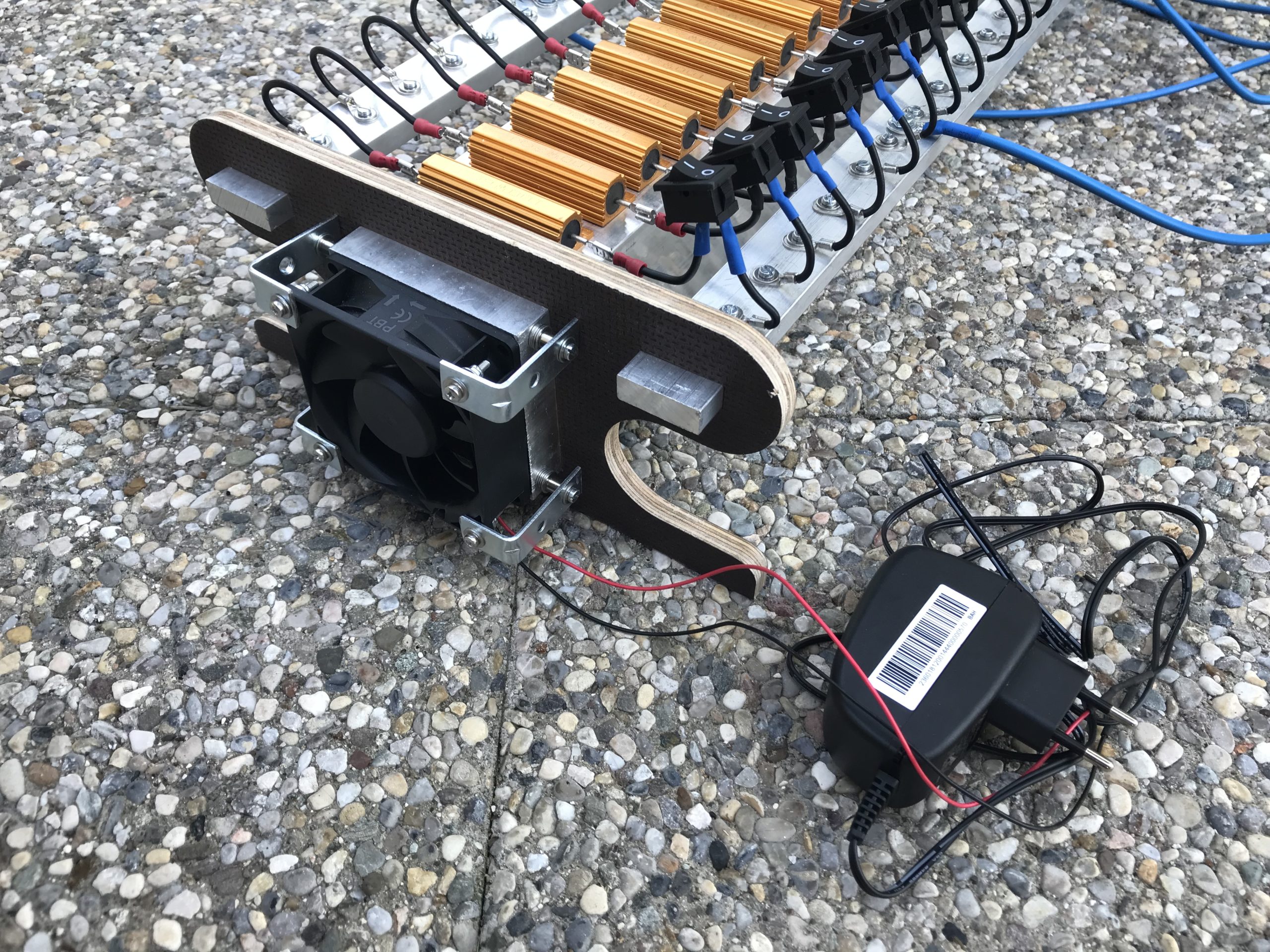
For determining the current capability of the switch, I built a test bench for load simulation. TBv1 consists of 35 power resistors (2 Ohm, 100W rated each) mounted on an aluminium tube with a fan on each end forcing airflow through it. The voltage supply is a Platinum grade PSU from HP, rated for up to 200A at 12V. It doesn’t matter if testing is done with 5V, 12V, 72V or 100V. Only the current flowing is decisive (I^2*R).

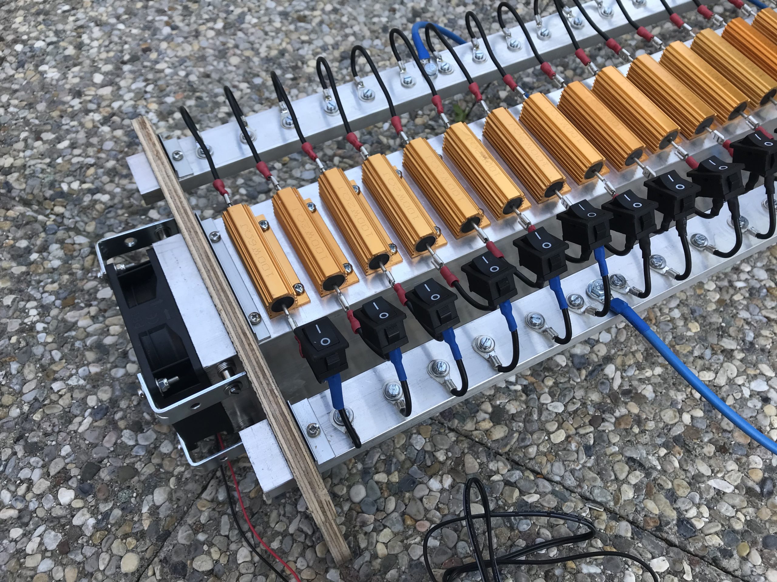
Some 2Ω resistors decided to show their insides combined with a weird smell during operation. They were replaced by 6Ω ones, because I didn’t order any spare 2Ω resistors (dumb me). Rated for 100W each, even without the aluminium tube they are mounted on. Only 72W were applied (12V^2/2Ω). Case-temperature was about 160°C (should be fine up to at least 250°C). I suspect the black plastic covers got soft nevertheless, and possible tension from the spade connectors opened them up. To be fair, they are the cheapest no-name ones from eBay. Worth the lecture I guess.

Looking for a way to somehow divide the dissipated energy, led to version 2 of the test bench using another 35x 12V/50W halogen lights in addition to the resistors.
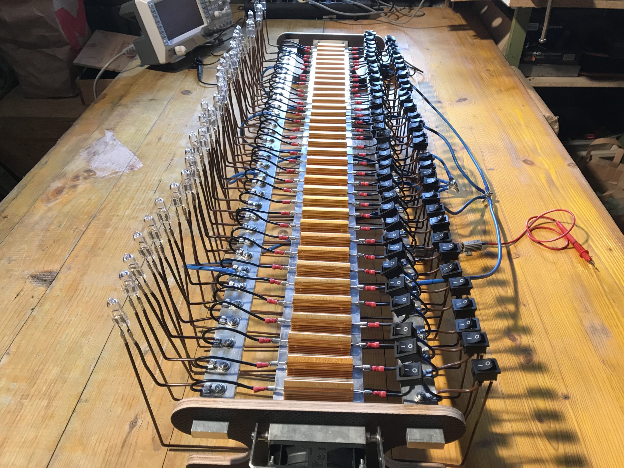
Since the resistance of cold coils of halogen lights is incredibly small and “cold-starting” them lets my PSUs collapse, they must somehow be preheated. Using a classic NTC in series with each lamp was one of the first thoughts. Ideally, the 25°C resistance of the NTC should be around 12V/(50W/12V), so the inrush current would equal the operating current of the halogen light. However, using them quickly adds up cost wise (~1€ each and according to initial calculations, even two in series per halogen lamp are required, so 70 NTC).
The budget version of this are normal shunt resistors I had lying around, connected to the positive supply voltage on one end and soldered to an old probe on the other end. Before switching the lamp on permanently, it’s preheated by current flowing through the shunt resistor, with the probe end supplying the lamp until the black rocker-switch is switched and the shunt then removed. I use a normal shunt resistor instead of an NTC, so I don’t have to wait for them to cool down and increase their resistance value again.
Even one halogen lamp is incredibly bright, therefore some coverage is necessary.


Temperature measurements on the switch during operation
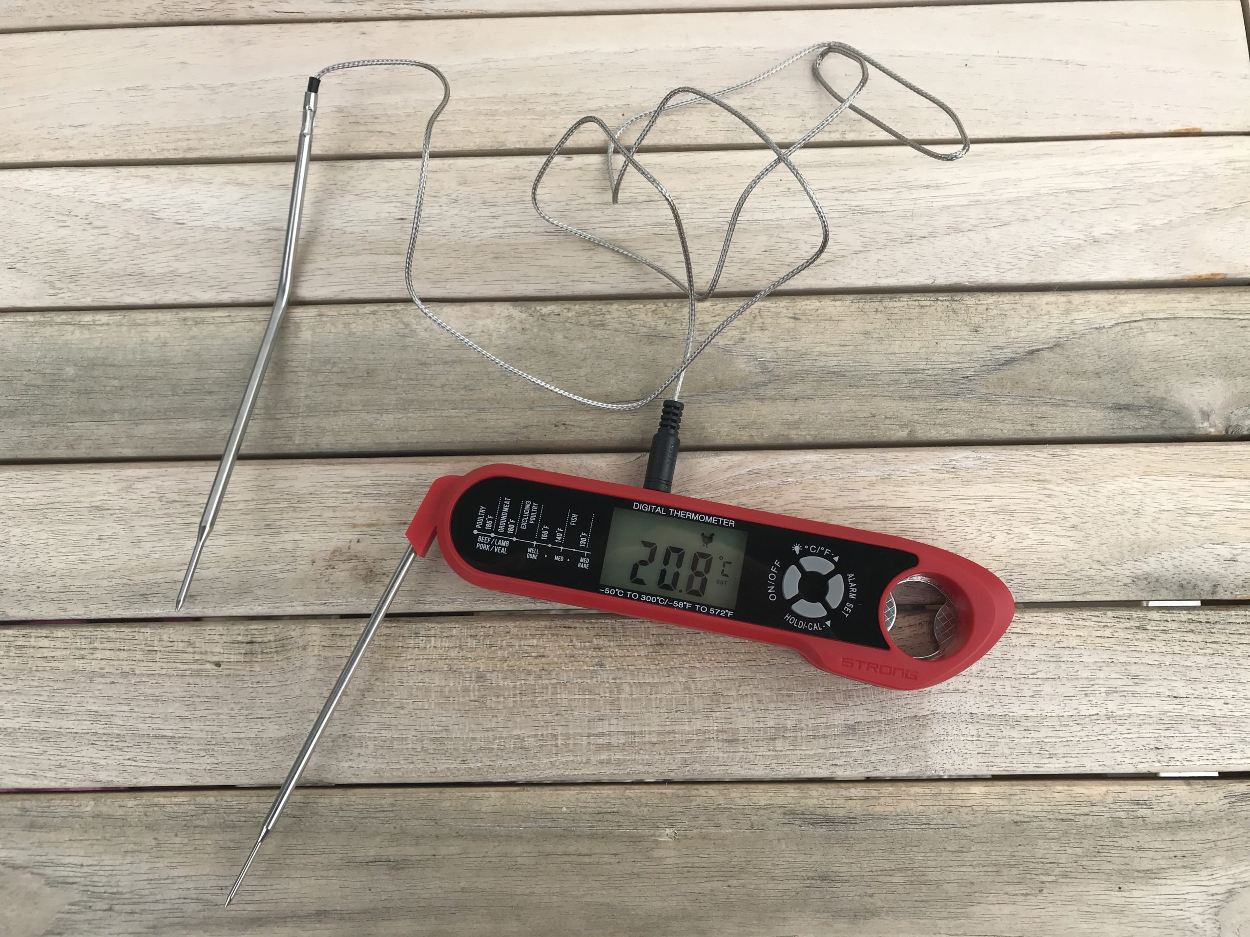
Many multimeters feature a temperature measurement option, however this feature is most likely based on the thermocouple principle (Seebeck effect, Type-K probes), which is only suitable for measuring voltage free surfaces.
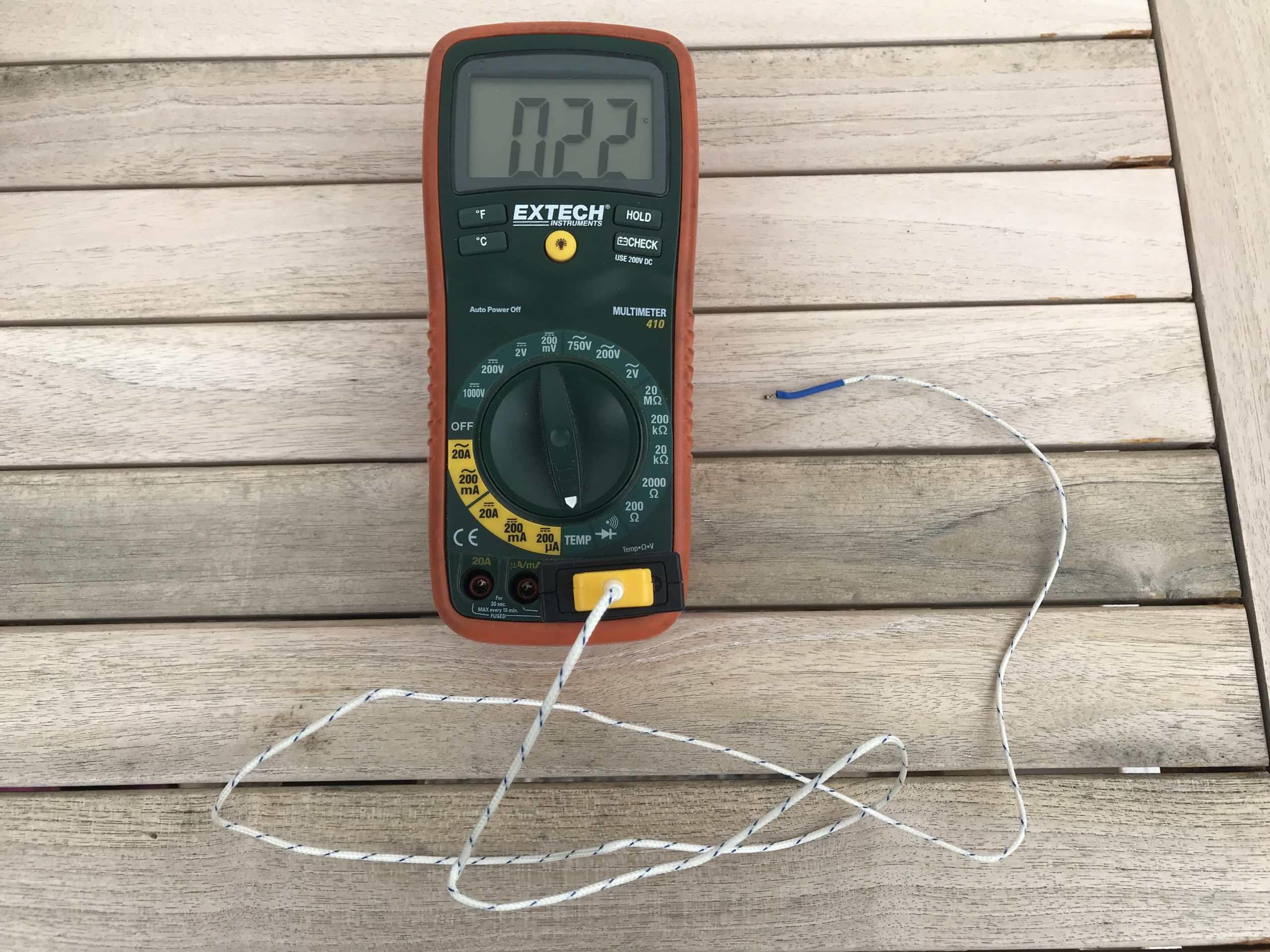
Infrared thermometers (Pyrometers) are not a great choice when it comes to low emission coefficients, like shiny metal surfaces (blank copper or aluminium). This can lead to wrong readings if the coefficient of the material targeted does not match the setting of the infrared thermometer. Many inexpensive devices have a fixed coefficient of 0.95 pre-programmed, while blank copper surfaces have an emission coefficient of 0.05 or something like that. However, they are great at measuring case temperatures of MOSFETs (black plastic packages).

The best option is to use e.g. a Pt100 or Pt1000 Resistance Temperature Detector (RTD). This temperature dependent resistor is encapsulated by a ceramic or metal case and can usually be utilized to measure temperatures of surfaces under voltages.
Passive cooling solutions have a coloured surface (black is not mandatory) to achieve a high emission coefficient (>0.9) for better heat emission into the air. Since I use blank copper, it’s basically just thermal capacity and not a heatsink per se. Copper can be treated with Nerofor to create a black copper surface. However I’m not sure on how much this would actually improve heat management since the circuit board is wrapped in heat shrink or if it is even necessary. Also, only certain parts of the copper should turn black (oxid layer) in order to still make good electrical contact with the cable lugs screwed onto it. I guess the overall benefits of Nerofor treated copper will be negligible and not worth the hassle.
Introduction to thermal considerations, calculations and limits
Goal is to measure or accurately estimate the operating junction temperature of the MOSFET. There are different approaches of doing so. For the sake of reliability, I set a healthy limit of 125°C for maximum  , also with the glass transition temperature of the PCB in mind. Joule losses of the PCB are neglected due to the mounted copper bars. Assuming equal current distribution through MOSFETs.
- Place a temperature sensor on top of the case, know the maximum junction to case thermal resistance at drain (datasheet) as well as dissipation power and calculate as a function of the currently measured case temperature
 according to
- Measure the temperature directly on the drain pins of the MOSFET (caution: voltage!) and add 10-15°C to it
- Measurement of temperature sensitive parameters e.g. threshold voltage. This is rather advanced.

The Joule-losses heat up the MOSFET, this in turn lets the ambient temperature rise (especially in a closed environment). The MOSFET will dissipate less and less heat due to the decreasing temperature difference to its surrounding environment. Case and Junction temperature rise and lead to thermal failure. A stable current rating must be determined to prevent this scenario. It is found, if the corresponding case and junction temperatures are not exceeded for permanent operation at that specific current value.
Determining the current that a single FET can safely carry
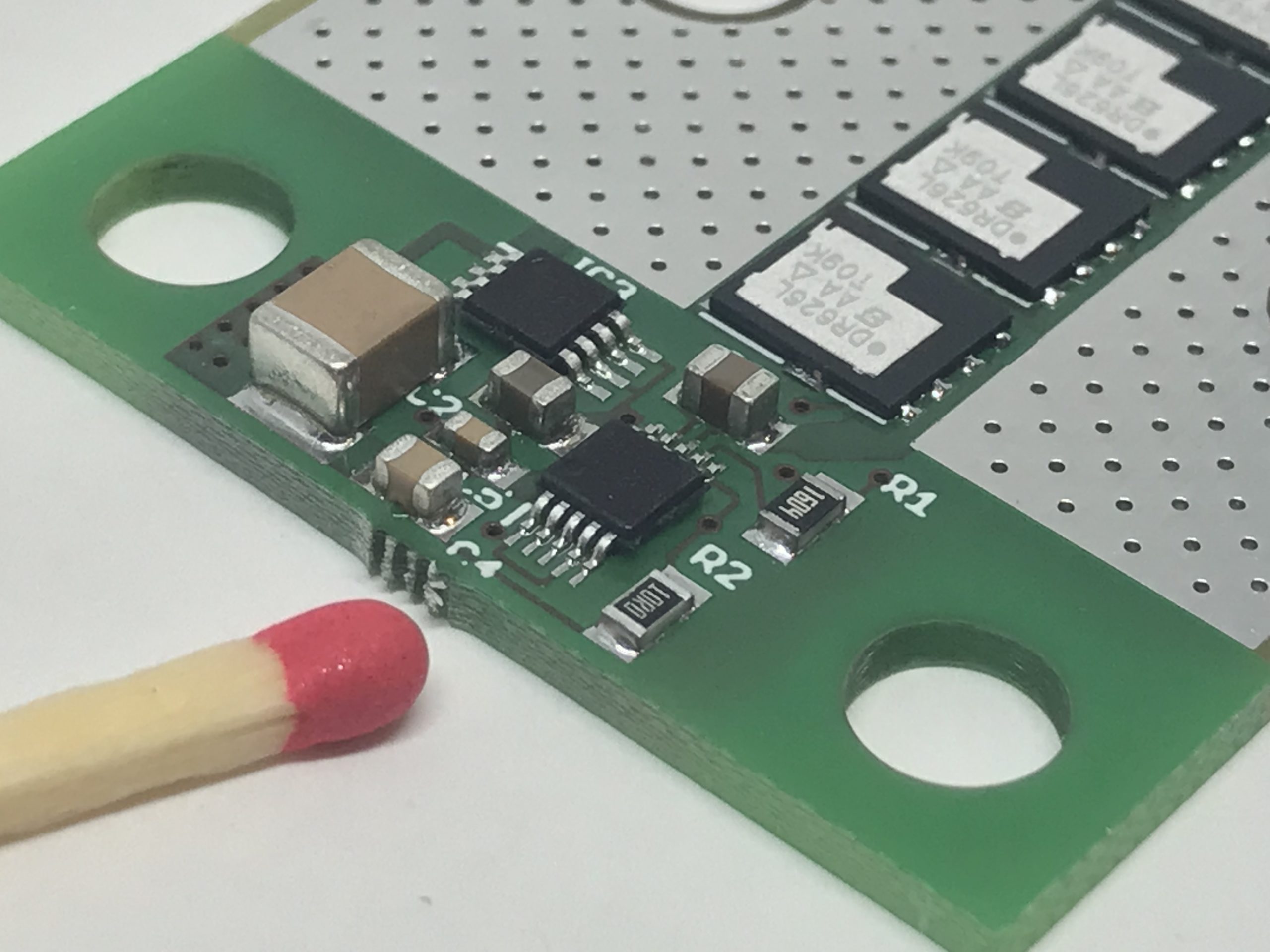
Looking at the SIDR626LDP-T1-RE3. Its package is a PowerPAK SO-8DC, typical  , maximum
  .
.
At this point I will omit the paragraph telling that the current ratings in the datasheet are just marketing nonsense and come straight to the calculation.
Maximum junction to ambient air thermal resistance 
Maximum junction temperature  .
.
Assuming the ambient air temperature is 25°C and junction temperature is 150°C results in a temperature difference of  .
.
Calculating dissipation power with those numbers:
(1) 
Typical but the maximum value is  . Furthermore, this value increases with rising temperature. At 150°C, the increases by a factor of 1.8 according to the datasheet, therefore now
  .
.
Using  , the current can be calculated:
(2) 
That is the maximum allowed current value without any cooling measures, where the FET (more specific the silicon) is just not melting yet. Beyond the maximum junction temperature the semiconductor becomes intrinsic, the dopants diffuse and functionality is lost.
However the package of the FET is still blazing hot since is at 150°C. With  , the temperature of the case will be
Assuming an ambient temperature of 40°C (e.g. inside a box or enclosure), then the maximum current value reduces to around 45A redoing the calculation above. You could then derate that value by 40-50% and you would be very safe.
Assuming you want to know the maximum allowed current where the junction temperature does not exceed 60°C for the above MOSFET without any cooling measures and at an ambient air temperature of 25°C. Maximum specified values (datasheet) are used instead of the typical ones for and  to cover worst case scenarios (“Monday MOSFET”). At 60°C the will be
(3) 
(4) 
(5) 
Again at  , the increases by 20% according to the datasheet.
Remember, this is without any cooling/heat sinks. The switch uses 8 of those MOSFETS for a maximum current of 200A with heavy copper bars mounted.

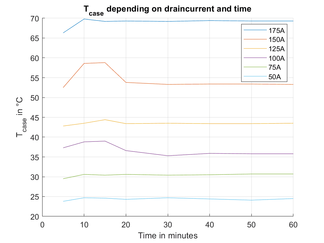
ScorpionLV v2 (60V)

Ad1)
MOSFET: SIR626DP-T1-RE3, worst case values = 125°C (=personal set limit)
 = 1.2°C/W
 =
=  =(200A/8 Mosfets)^2*1.7mOhm ≅ 1.1W
 = –
= – * ≅ 124°C
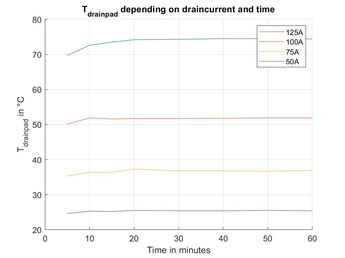
So if we measure 124°C on the case near drain, the set thermal limit for is reached. To account for measurement and calculation deviations, I’ll lower the value for the maximum acceptable case temperature from 124°C to 120°C. Many semiconductors are specified up to =175°C. Everything below 50°C is considered cold.
The RTD probe measures the temperature of the MOSFETs drain pad, while the IR thermometer measures case temperature. Current is increased in 25A steps, starting from 50A while monitoring temperatures.
The diagram below shows case temperature as function of time for a specific current value (50A, 75A, 100A, 125A, 150A,…).

ScorpionHV v2 (120V)
Same test procedure as above.
The FDMS4D0N12C is more expensive, does have similar SOA and a maximum of 4mOhm at 120V maximum  (the 60V used before have max 1.7mOhm). Therefore, the current capability will certainly be lower.
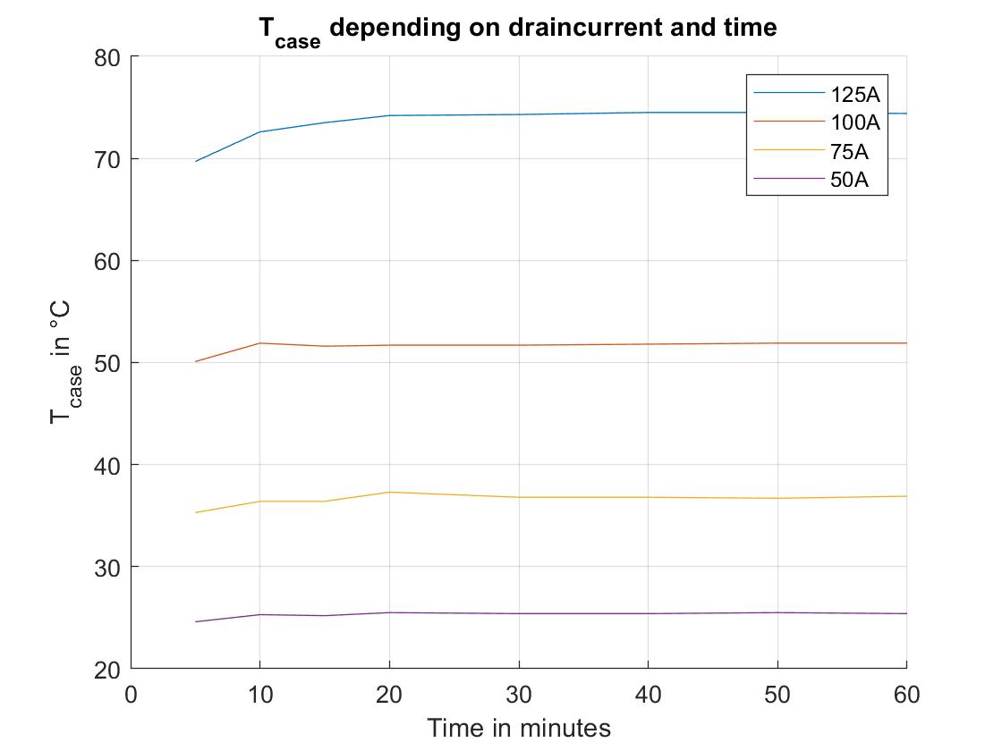
This time, I also measured the voltage drop across the switch (drain-side copper bar to source-side copper bar) to approximately measure the dissipation of power across the whole switch unit (U*I). An approximate theoretical dissipation power can also be calculated by knowing the load current and only using the theoretical maximum channel resistance of eight MOSFETS paralleled.

Capacitive load capability
In order to control the inrush current, either charging up through a beefy resistor in side branch and closing the main current path after  , or controlling
  is possible. The current equation of a capacitor is .
Using dV/dt limiting for precharging, the inrush current is proportional to the amount of capacitance to be precharged, while the time duration of the inrush current is dependent on the final operating voltage. So high capacitance and high voltage combined is the most delicate scenario because it means “high” and “long” inrush current which must still be inside SOA. For this purpose, I built a 15 000 uF/160V capacitor bank consisting of ten 1500uF/160V electrolytic capacitors.
Charging/discharging tests can either be performed manually or using relays controlled by an Arduino Nano.


Using Single Shot functionality on the oscilloscope, the rising voltage of the capacitor bank can be viewed.
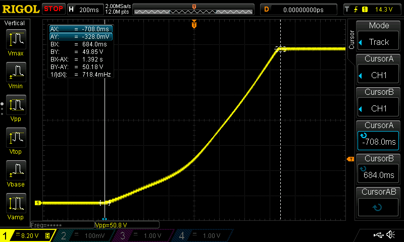
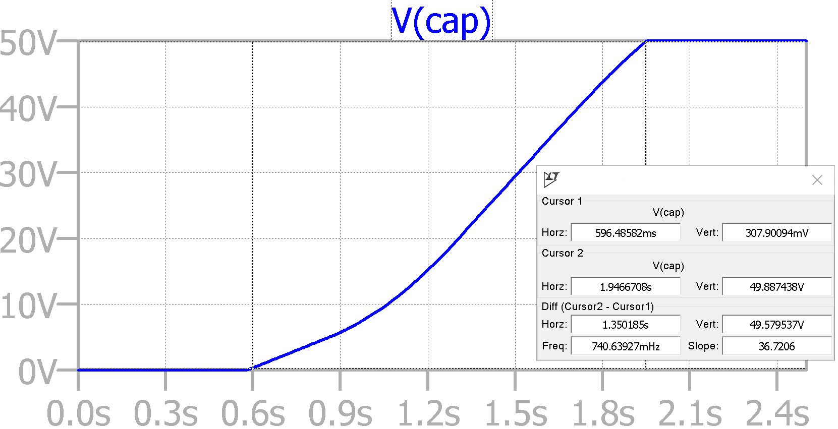

The inrush current lasts about 1.1s (0.5s to 1.6s) with a maximum of around 110mA (equal current distribution through all MOSFETS). So let’s have a look at the SOA diagram of the MOSFETS used (SIR626DP-T1-RE3). The Drain-Source voltage together with the corresponding Drain-Source current allows for an estimation where we are moving around.

Moving from the right corner (Spirito region) to the left within 1.1s. Everything inside DC area (>10s), so no problemo.
Switching on and off thousands of times for testing would be a pretty boring task, better automate that. The resulting test bench is shown below.

Relays are great. You don’t have to worry about threshold voltages and can switch potential free. However, their ratings are science in itself, resulting in the Arduino Nano controlling a small 5V logic level relay which then drives a larger 12V relay with appropriate DC ratings (>120V and current >120V/30Ohm). The control input of the switch is hooked to a third relay imitating me pressing the LED switch. A counter counts the On/Off switching cycles performed up to a programmed number (e.g. 1000). The delays between the switching actions need to be adjusted to the time constants occurring in the circuit (charging with limited inrush current and discharge through resistor). The SOA values are considered Single pulse, so an extra delay between On/Off cycles does certainly not hurt to allow heat being transported away from the silicon to the copper bars.

Quiescent current
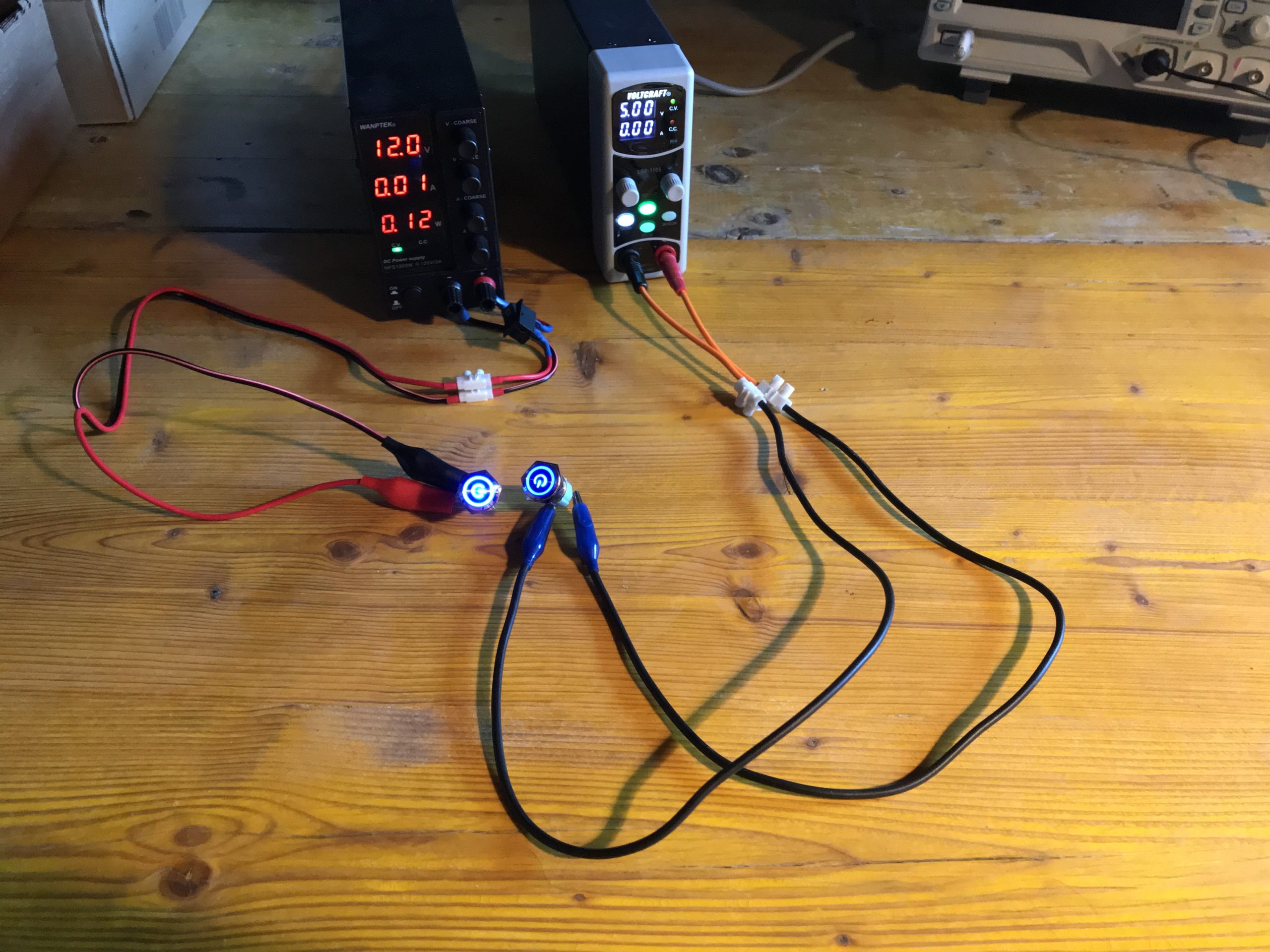
The quiescent current is the current flowing while the switch is off (unwanted characteristic obviously). Although usually in the microampere range, it can still be important depending on the application, e.g. when powering a device by a permanently connected battery.
By connecting a voltage source to the switch in off-state and using an ampere meter in the power path, the quiescent current can be measured. My goal was 10 µA maximum, which was met. Since the capacitor bank is connected, this current also includes the leakage current of the MOSFETs in off-state, however this contribution is usually more than negligible.


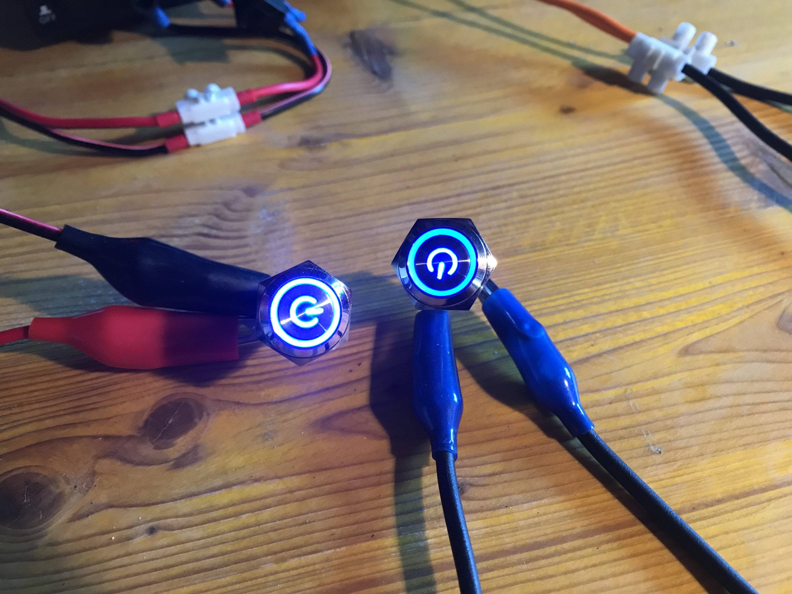
LED Switch
By connecting an external latching SPDT type switch (LED illumination optional) to the JST-GH terminal, the power-switch can be controlled comfortably. The blue light with the power symbol will light up if the switch is on.
Standard configuration for the external SPDT switch is:
- Switch pressed = ON
- Switch not pressed = OFF
However, by changing two of the wires it is also possible to operate it the other way around:
- Switch pressed = OFF
- Switch not pressed = ON
Which leads to more reliability in vibration heavy environment.
Using 5V or 12V for supplying a 12V-rated LED switch shows no disqualifying difference in terms of brightness in my opinion.
Changes from V1 to V2
- Doubled the number of MOSFETS (from 4 to 8), physical PCB size remains the same, the additional MOSFETs are mounted on the back
- Using 3-pin JST-GH instead of 5-pin JST-GH for easier change between “ON=pressed” respectively “ON=not pressed” mode


Experimental add-ons
Passive cooler
As already mentioned, the blank copper bars function as screw terminals and add thermal mass but aren’t fulfilling the function of a passive cooler due to the low emission coefficient of blank copper. Treating the copper with Nerofor to make it black would increase heat emission, the contacting area of the cable lug and the soldering areas should be left blank, however I tried a different idea.

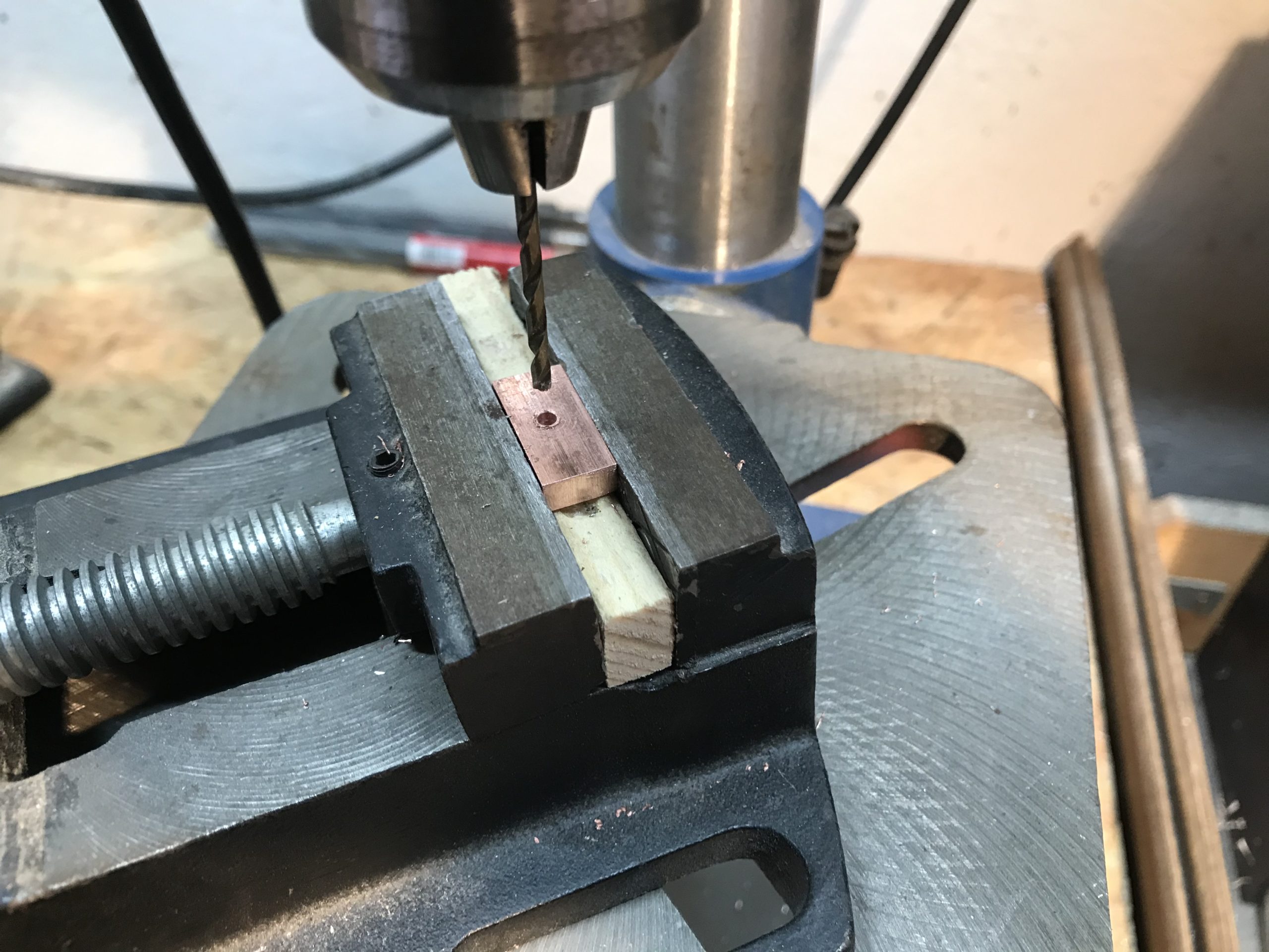
Drilling clean holes in thin sheet metal can be quite a challenge, but they are hidden afterwards anyway.
In-line fuse
The kind of fuse pictured here usually has a voltage rating of 58V. This spec gets important when the fuse blows to make sure the connection stays interrupted.


Miscellaneous
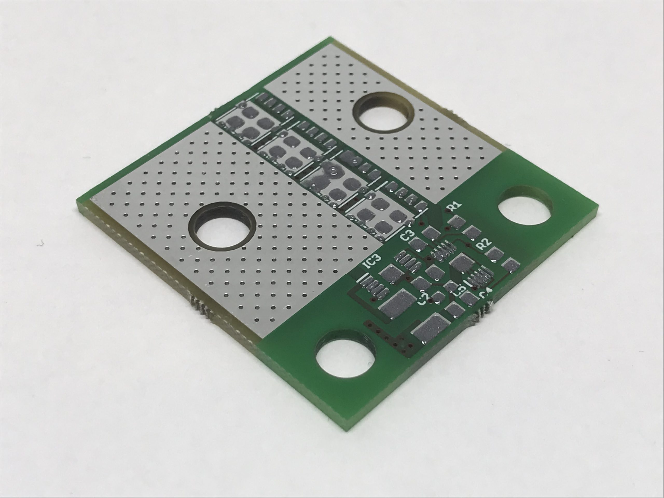
- To prevent cracking of the MLCCs, their footprint orientation with respect to mounting holes, screw terminals or PCB dimensions plays a major role. You generally don’t want the “long” side of the capacitor (so e.g. the 0.06″ side of a 0603 cap) to be equally aligned with the direction where the PCB could mechanically bend. Regarding this PCB here, the prone axis would be the one going from the drain to the source copper bar. However, the return path of the current is a 10mmx2mm copper bar going in the same axis and therefore provides mechanical stability.
- The return current path (10x2mm copper bar) is going over the electronics located on the other side of the PCB. To prevent voltages induced by inductive coupling (U=L*di/dt), no loops should be routed. The di/dt of the current flowing shouldn’t be high, since the expected big capacitors at the input of the load act as a buffer.
- Thermal expansion of copper. A copper pipe going through a temperature difference of 50°C (e.g. heating up from 20°C to 70°C) will expand 0.82mm per meter. The copper bars soldered and screwed on the blank areas are 21.5mm on their longest side, so they will expand 0.018mm. This should be no concern regarding cracks in the solder.
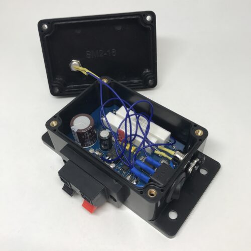
More pictures