The two external capacitors are a crucial part in setting the correct frequency in a Pierce oscillators circuit. This circuit is often used as external clock source for microcontrollers.

 is load capacitance specified in the datasheet of the crystal resonator and can be calculated according to the formula below.
(1) 
Most likely you will choose the same value for  and
and  , with
  being the input + stray capacitance. Values between 3 pF and 7 pF are usually chosen for according to literature. It depends e.g. on your PCB layout and the crystal case. Usually a “good guess” is made on that value and later verified on the prototype design.
Example:
Load capacitance 
Stray capacitance 
Same value should be chosen for and
(2) 
Therefore 
In simple words: Subtract the assumed stray capacitance from the load capacitance stated in the datasheet and double that value.
C0G (NP0) type ceramic capacitors are the first choice for and due to their temperature stable dielectric. Temperature drift is usually less than ±0.3% C from -55°C to +125°C with negligible capacitance drift and hysteresis.
Another parameter is the ESR of the crystal. It determines how quickly and easily the crystal sarts oscillating, where lower ESR. Basically, how hard it needs to get “hit” with current to start oscillating. Low ESR means more reliable startup.
Experiment description
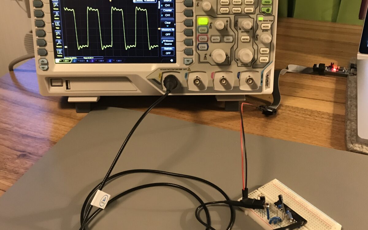
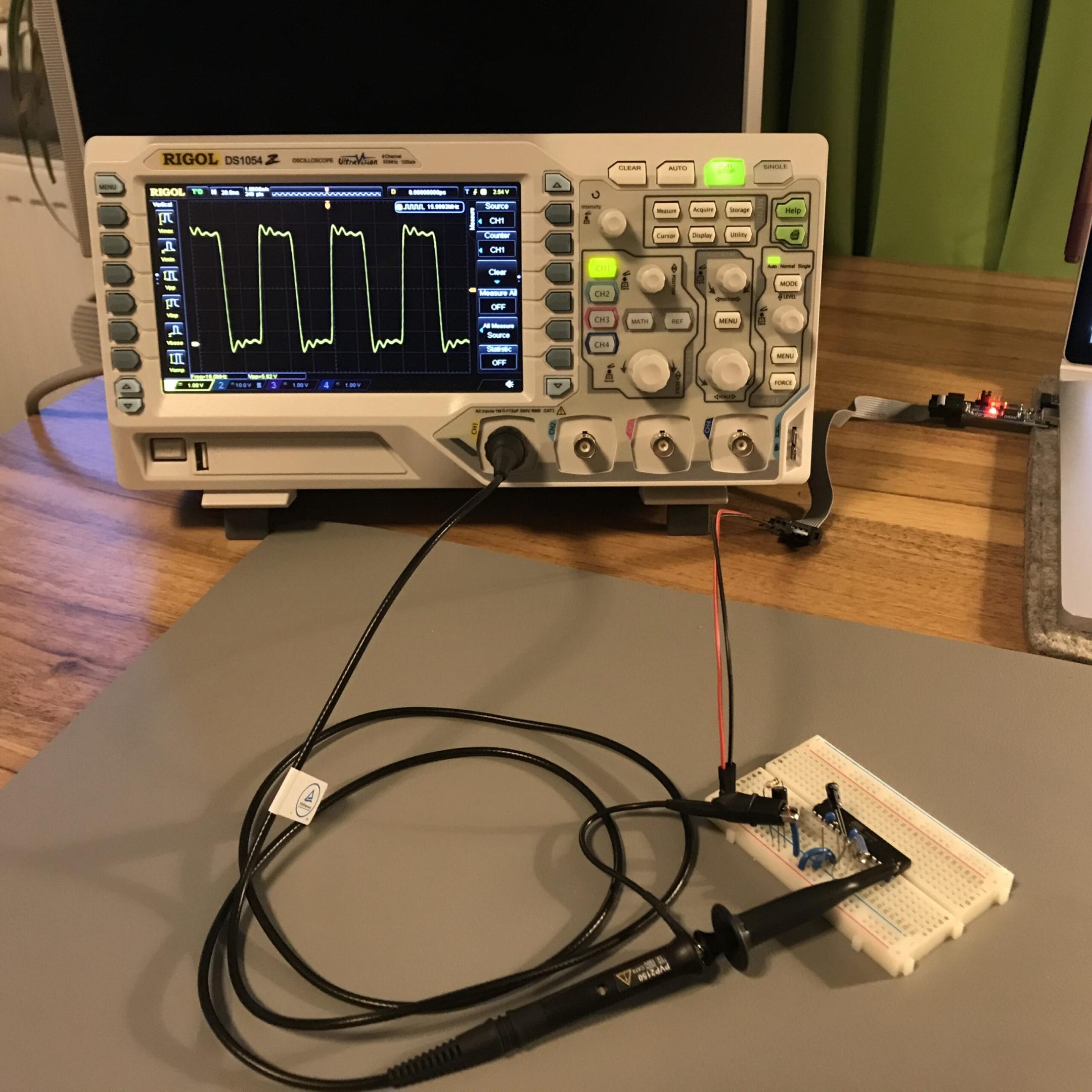
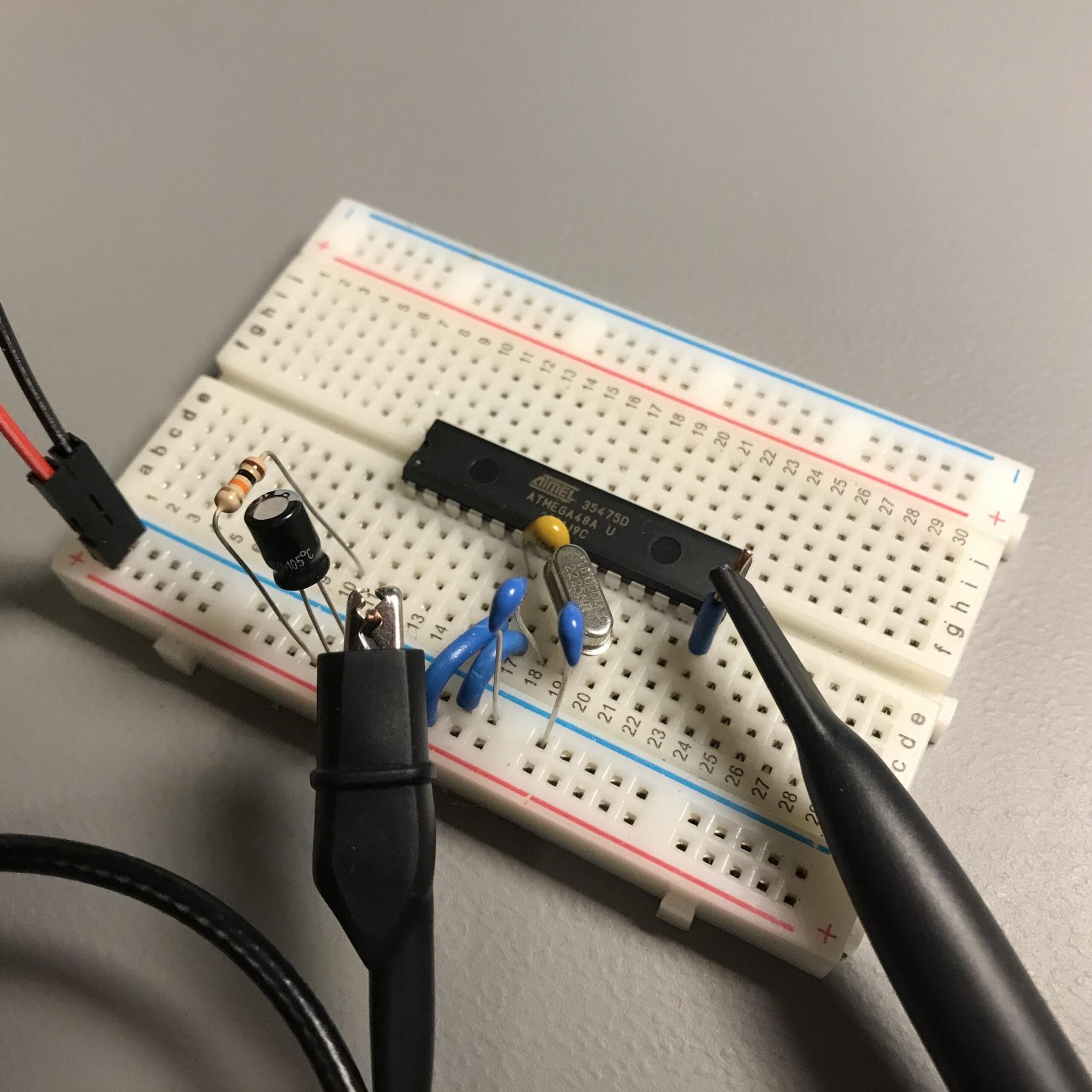
To show the impact of wrongly chosen capacitors, different crystal resonators and capacitors are set up as external clock source for an ATmega48A microcontroller wired on a breadboard. The clock frequency is measured with an RIGOL DS1054Z digital oscilloscope + RIGOL PVP2150 probe (150MHz bandwidth at 10:1). Connecting the oscilloscope probe directly onto the external resonator will change the capacitance of the circuit (probe capacitance) and therefore the clock frequency. To measure the unaltered clock frequency, the CKOUT fuse bit is set to output the clock on PORTB0 of the ATmega48A. Complete setup is shown in the picture below.
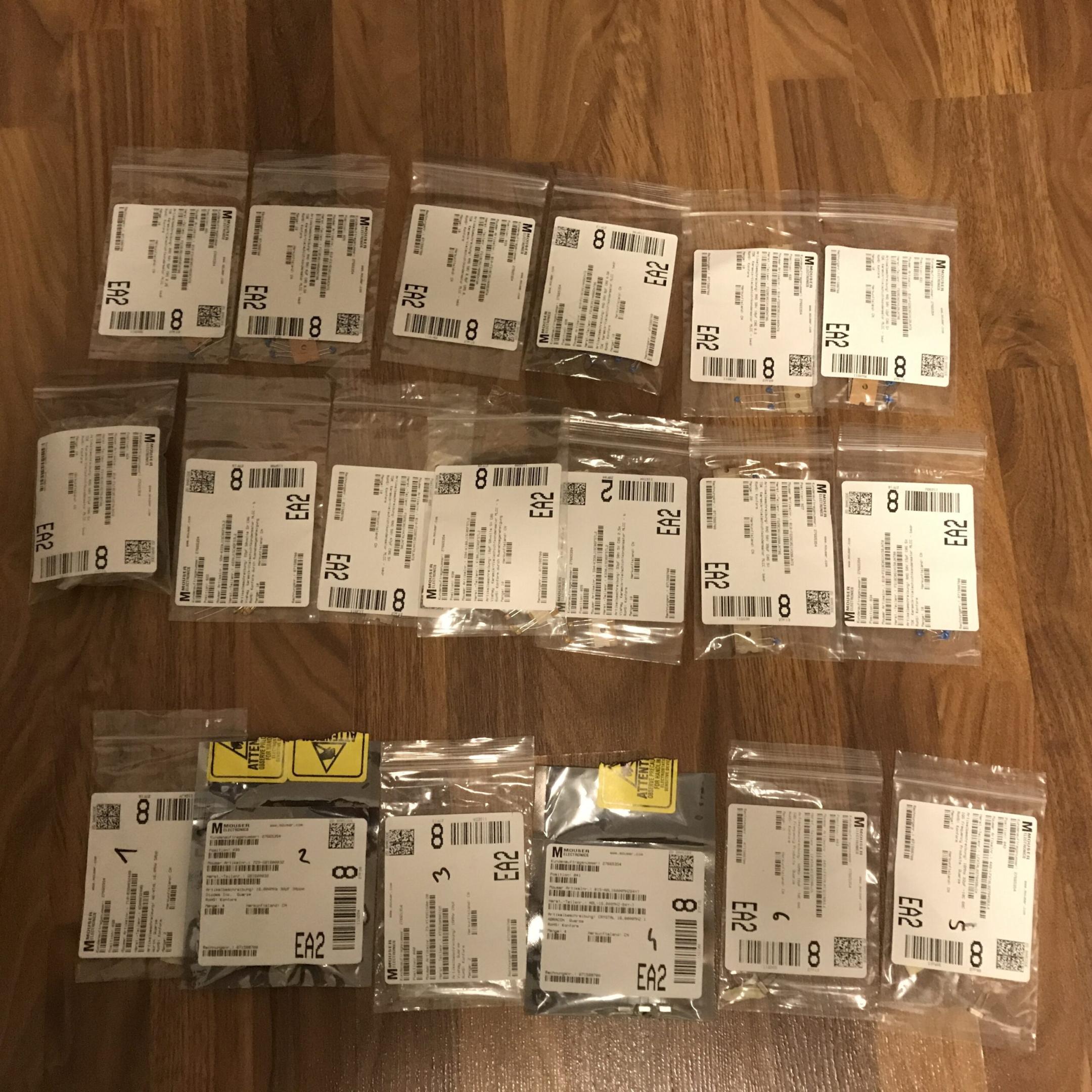
Each crystal resonator was tested with the capacitors listed in the table below (all C0G, 5%, type is radial leaded, TDK and Vishay).
| Capacitance in pF | Manufacturer part number |
| 5 | FG18C0G1H050CNT06 |
| 6 | FG18C0G1H060DNT06 |
| 6.8 | FG18C0G1H6R8DNT00 |
| 8 | FG18C0G1H080DNT06 |
| 10 | FG28C0G1H100DNT06 |
| 12 | FG28C0G1H120JNT06 |
| 15 | FG18C0G1H150JNT00 |
| 18 | K180J15C0GF5TL2 |
| 22 | K220J15C0GF53L2 |
| 27 | FG18C0G1H270JNT00 |
| 33 | K330J15C0GF5TL2 |
| 39 | FG28C0G1H390JNT06 |
| 47 | FG28C0G1H470JNT06 |
| 56 | FG18C0G2A560JNT06 |
Setup and preparation
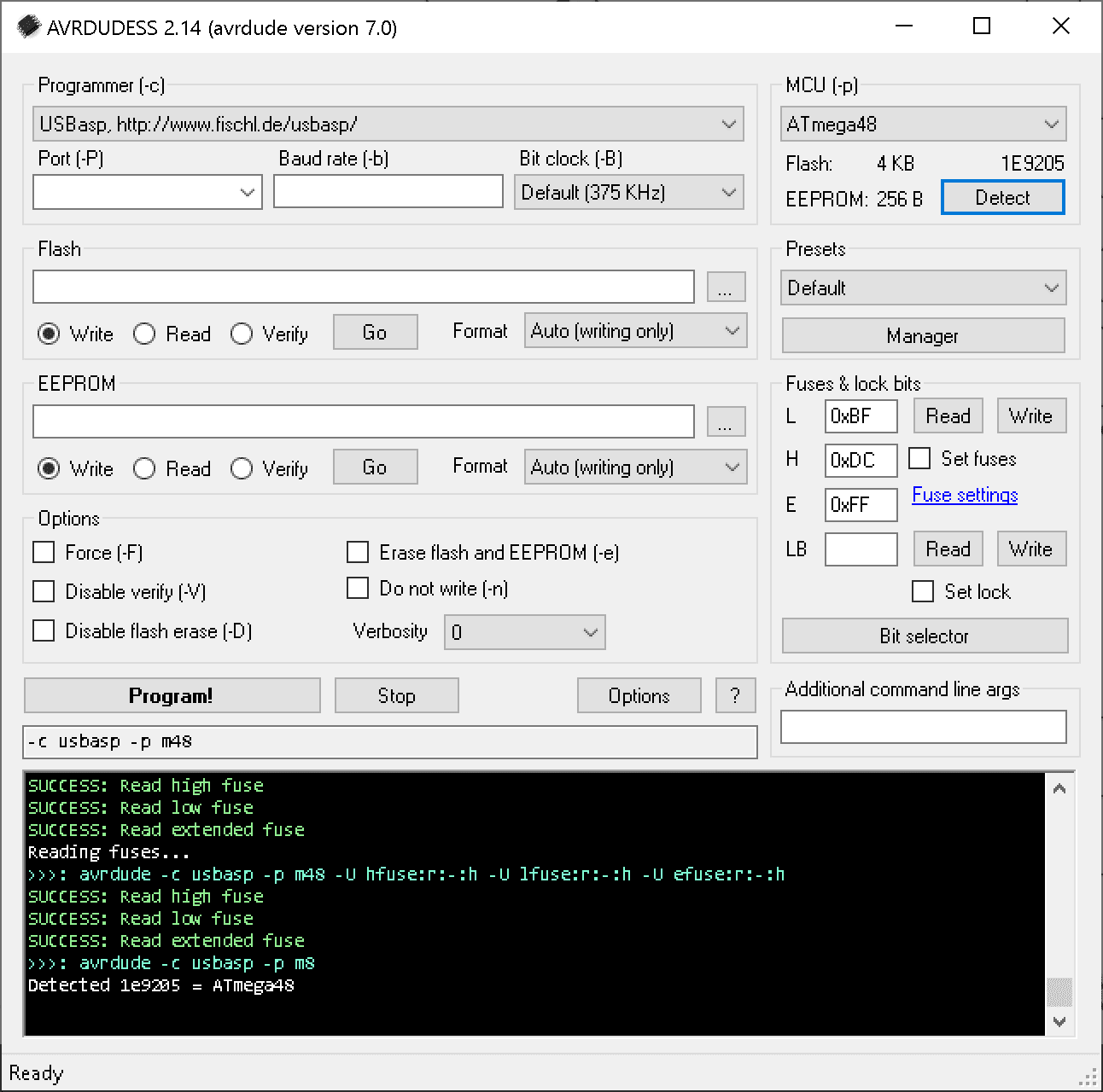
Fuse bits were set accordingly (L: 0xBF, H: 0xDC) to output the clock on PORTB0 among other configuration parameters. Factory setting was 0x62 for the low byte and 0xDF for the high byte.
Flashing was done using USBasp programmer.
The oscilloscope was in idle for 30 min to warm up, the probe was calibrated with the onboard 1kHz square wave signal. 10x divider setting was used on the probe. Instead of the frequency measurement option, the counter function is used, because it is more accurate. Room temperature was 22°C.
For a first evaluation, a random crystal resonator was chosen and connected to the circuit, frequency was measured with the biggest and smallest capacitor available (5pF and 56pF), to determine if there is even a difference in frequency observable and measurable with the current setup and available equipment.
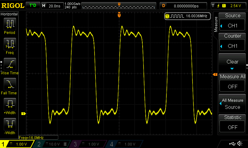
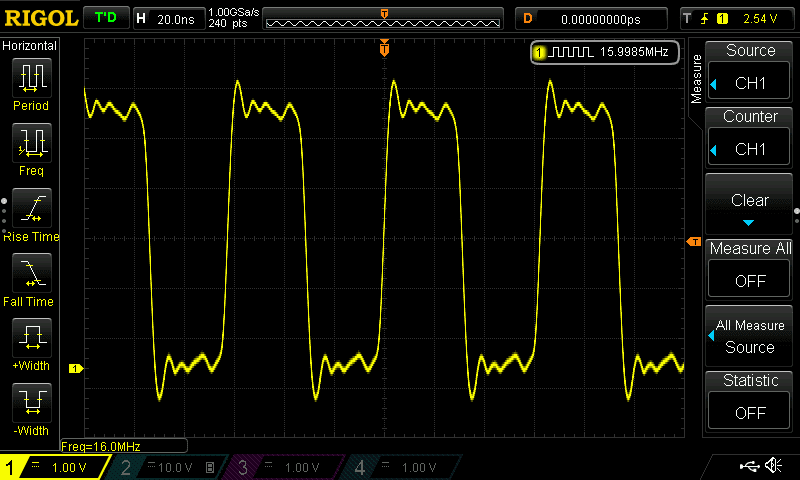
The difference in frequency observed was around 5.1 kHz.
Then the lead wires of the capacitors were cut shorter but no difference in frequency or signal form was observed.
XTAL1
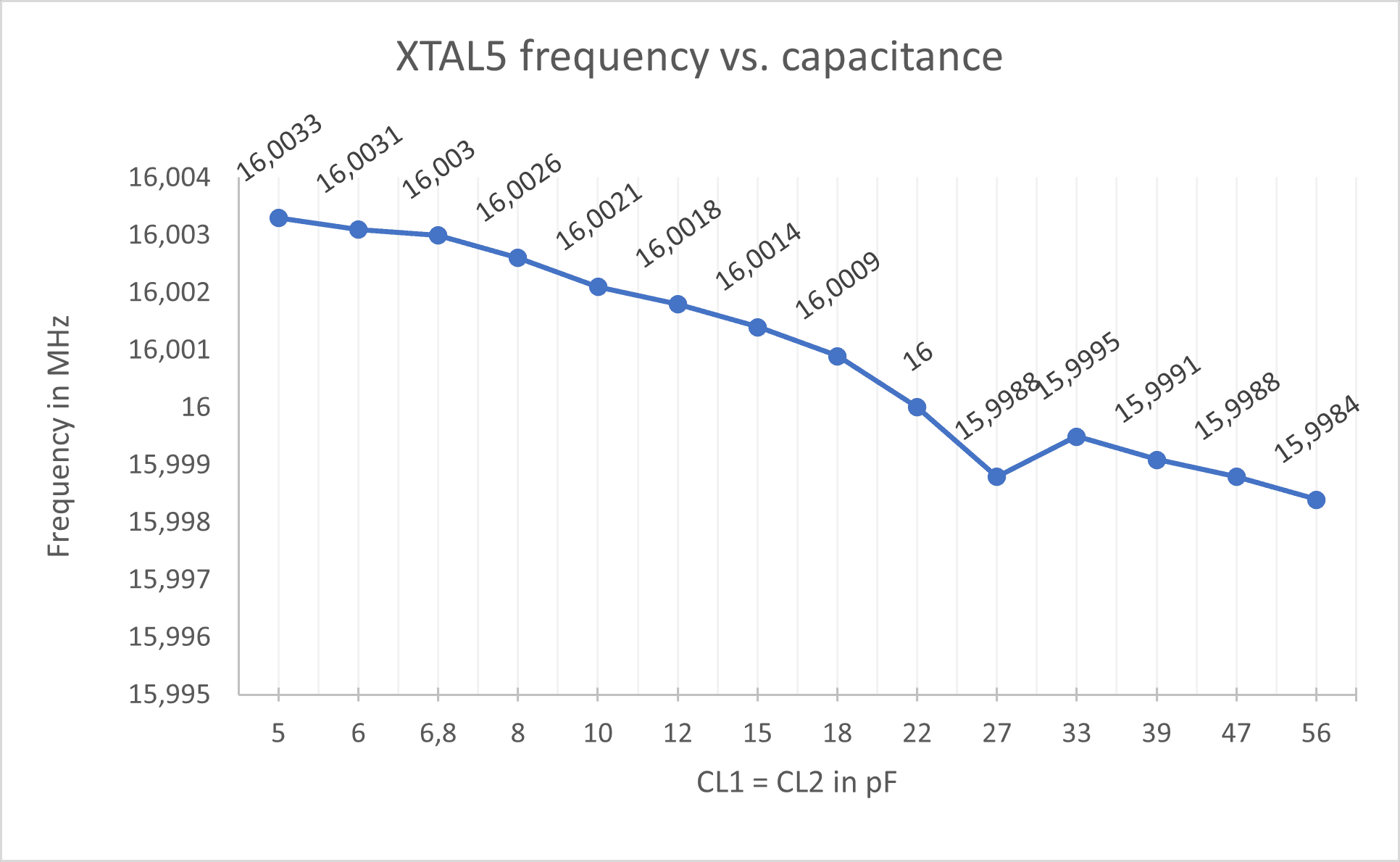
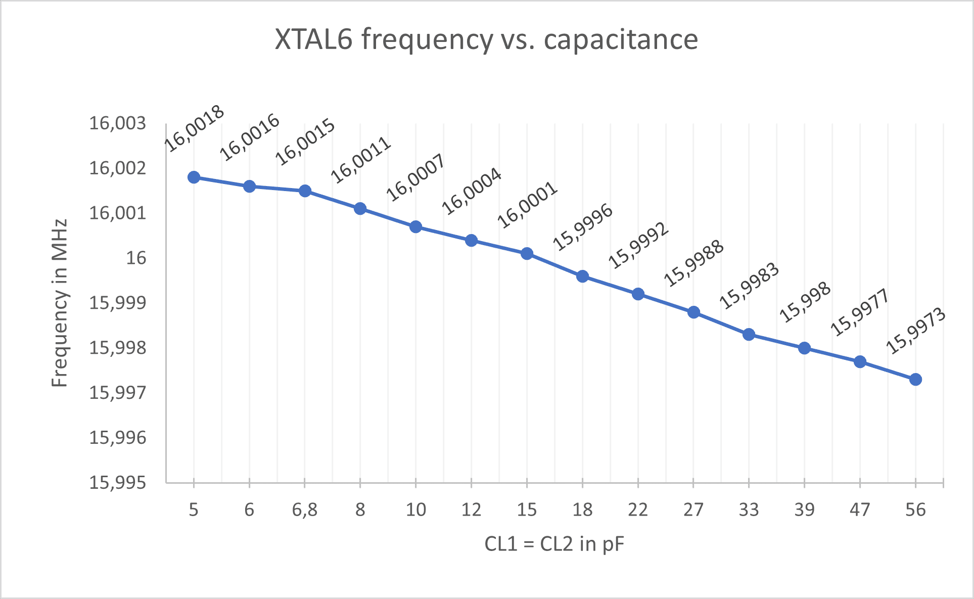
The x-axis represents the rated capacitance of each of the capacitors used (not the total load capacitance). That means two 5pF capacitors were inserted, the corresponding frequency measured, then two 6 pF capacitors were inserted, frequency measured again and so on according to the table above.
| Frequency: | 16 MHz |
| Load capacitance: | 30 pF |
| Manufacturer: | Wurth Elektronik |
| Mfr. No: | 830003240B |
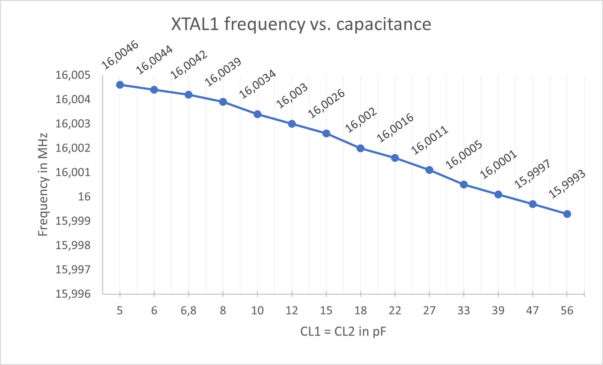
The closest value to 16 MHz is 16.0001 MHz when using two 39 pF capacitors, so the parasitic capacitance equals around 10.5 pF in this setup according to the formula above. This is a high value but not surprising since everything is mounted on a breadboard.
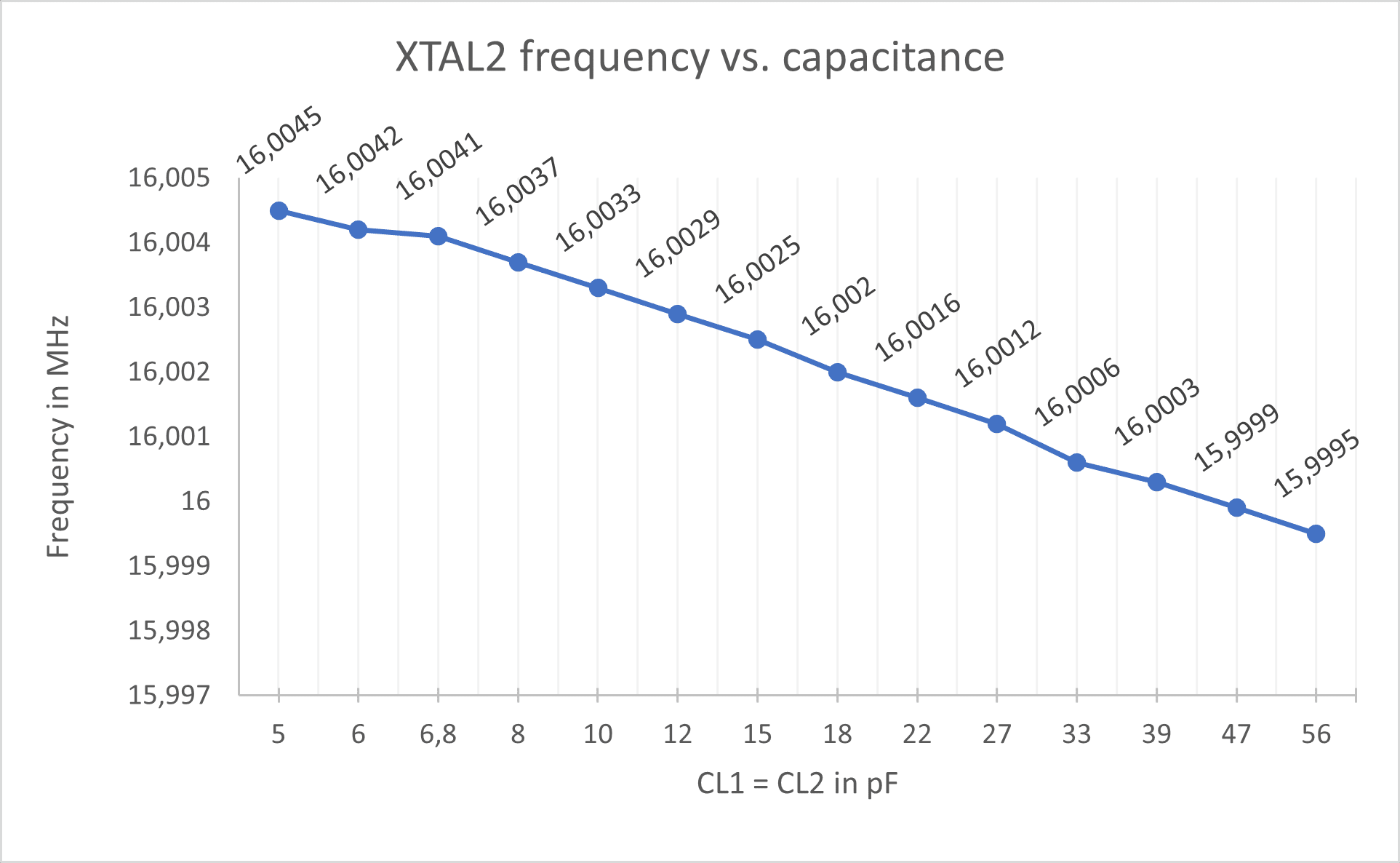
XTAL2
| Frequency: | 16 MHz |
| Load capacitance: | 10 pF |
| Manufacturer: | Diodes Incorporated |
| Mfr. No: | GB1600032 |
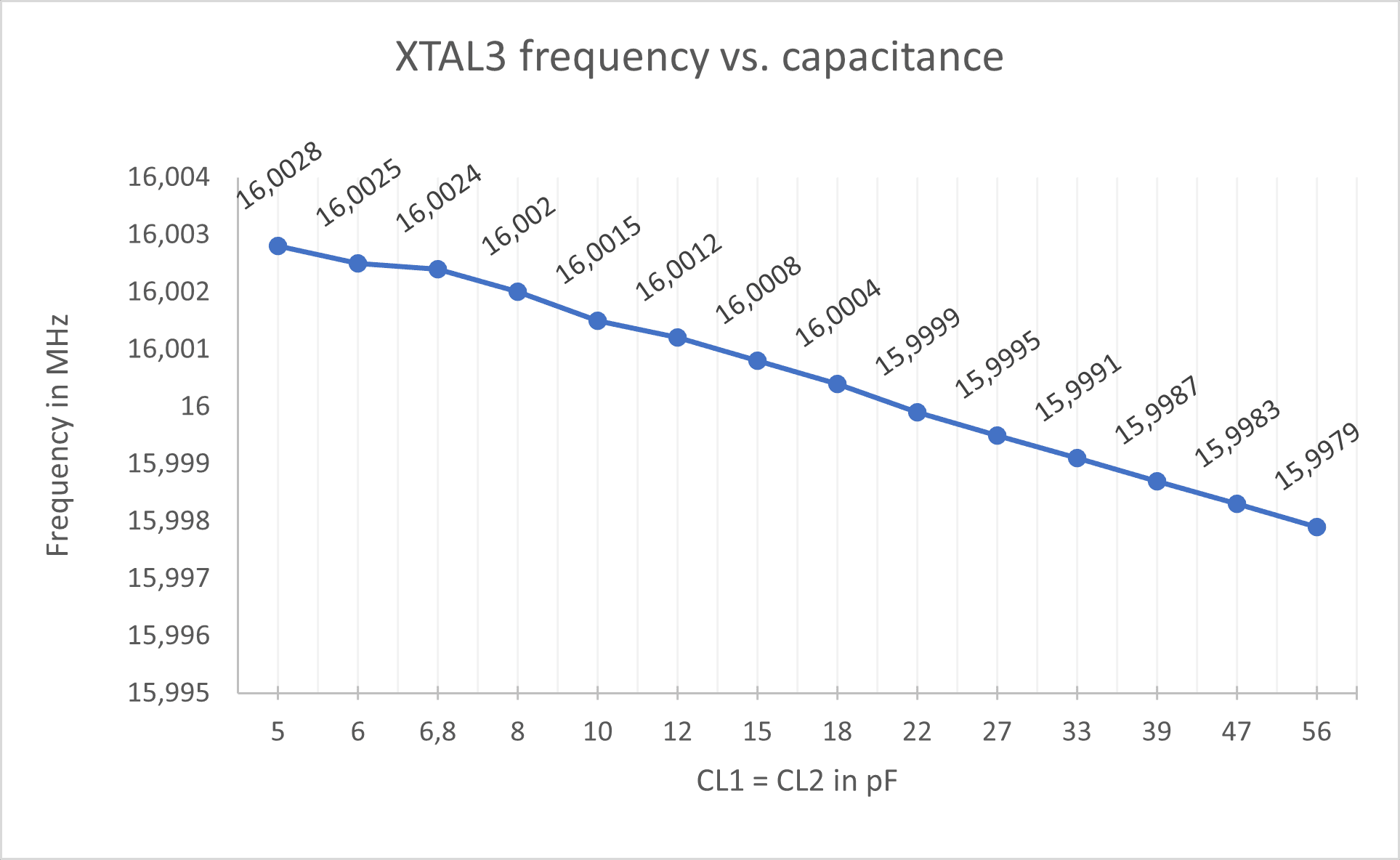
XTAL3
| Frequency: | 16 MHz |
| Load capacitance: | 20 pF |
| Manufacturer: | Vishay/Dale |
| Mfr. No: | XT9S20ANA16M |
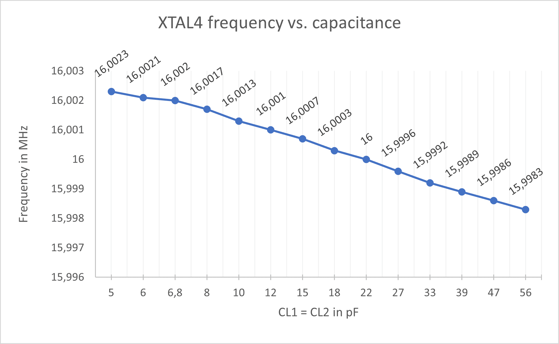
XTAL4
| Frequency: | 16 MHz |
| Load capacitance: | 18 pF |
| Manufacturer: | ABRACON |
| Mfr. No: | ABL-16.000MHz-B4Y-T |
XTAL5
| Frequency: | 16 MHz |
| Load capacitance: | 22 pF |
| Manufacturer: | IQD |
| Mfr. No: | LFXTAL027945Bulk |
XTAL6
| Frequency: | 16 MHz |
| Load capacitance: | 16 pF |
| Manufacturer: | IQD |
| Mfr. No: | LFXTAL013224Bulk |
A word on solderless breadboards
Using breadboards for this experiment is certainly not the optimum. Parasitics, leakage, poor reliability making it not an attractive choice, even for prototyping. You invite unnecessary extra problems in your design. A circuit working on a breadboard is also not automatically guaranteed to work on a PCB. Maybe the additional parasitic resistance, capacitance and inductance will prevent oscillations that would occur on a PCB or the other way around, they get components to oscillate, e.g. amplifiers.
A better way for this experiment would be a dedicated PCB like in the real product. Downside are the increased time effort (design, soldering etc.) and financial expenses (PCB production, time spent for the development), so probably better spent on a different project since this experiment is just due to personal interest in the topic.
The parasitic effects remain the same through the experiment because only the capacitors are replaced and the rest of the setup is unchanged. So at least a general trend should be recognizable.
Parasitics
The solderless metal contacts of the board have a certain parasitic capacitance to each other, around 2-3pF row to row, which is an issue for oscillator circuits. Even when omitting the two load capacitors on the pierce oscillator, the oscillator often still worked in the above experiment.
The illustration below shows the capacitance between the rows of the breadboard. It was measured with the DER-EE DE-5000 LCR meter using SMD tweezers. After performing calibration, one probe was placed in the leftmost row (red socket) while the second probe was placed successively in the next rows (blue socket). Pitch is 2.54 mm. Measurement was performed with 1 kHz, 10 kHz, and 100 kHz frequency.  results are written in the table below. The measurement with 100 Hz produced very fluctuating results and was therefore omitted.
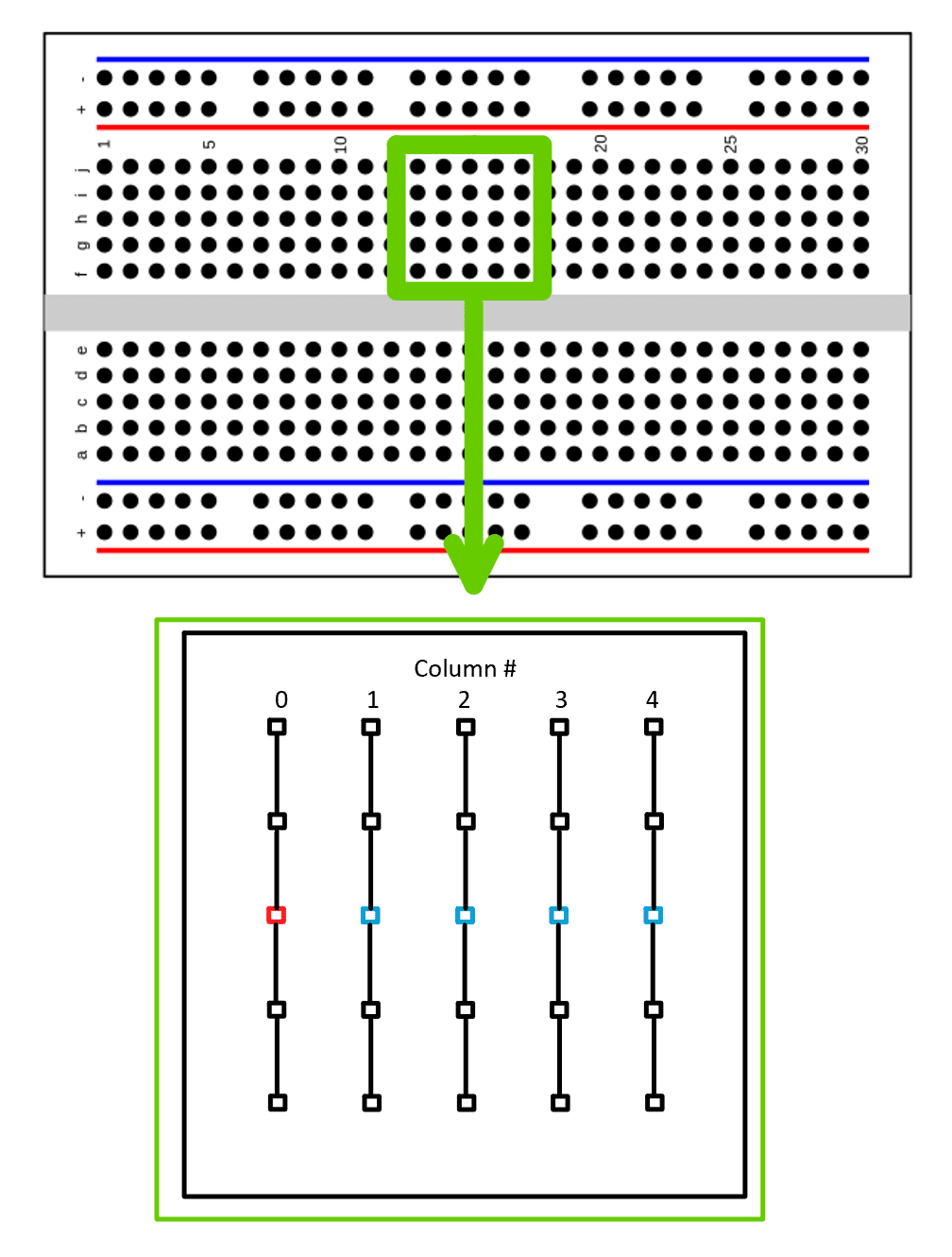
| fmeas | Column 0 to 1 | Column 0 to 2 | Column 0 to 3 | Column 0 to 4 |
| 1 kHz | 2.6 | 1.4 | 1.1 | 0.8 |
| 10 kHz | 2.61 | 1.52 | 1.09 | 0.84 |
| 100 kHz | 2.65 | 1.60 | 1.12 | 0.87 |
Capacitive coupling between traces or jumper wires is usually tiny, the parasitic inductance (nH range) on the other hand is often much more of a problem especially in digital circuits due to magnetic coupling causing cross talk if there is no close by power or ground return path available, then the closest signals will be used as return path.
Additionally, big loop areas and poor signal and ground return paths due to all the jumper wires used are awful and introduce ringing at improper or missing decoupling measures. It also opens all doors for  and ground bouncing. High contact resistance is another negative aspect, especially on older breadboards, where wires have been plugged in and out many times loosening up the connection.
On a PCB, you usually get yourself a free shunt capacitor when using big ground and power planes with the FR4 acting as dielectric, which is very handy.